Smart Home PCBA Manufacturing: Modules, Testing and Quality Control
Introduction
Smart home devices rely on printed circuit board assemblies (PCBA) to provide connectivity, sensing, power management, and intelligent control. From smart lighting controllers and connected thermostats to door sensors, smart plugs, and home gateways, each product depends on electronic assemblies that meet its functional, mechanical, and reliability requirements.
Manufacturing these assemblies involves more than mounting components onto a printed circuit board. Wireless performance can be affected by PCB layout and antenna placement, miniature components require appropriate assembly processes, and electrical or functional testing must reflect the intended application.
For original equipment manufacturers (OEMs), product developers, and procurement teams, selecting the right electronics manufacturing services (EMS) partner is an important part of bringing a smart home product from prototype to volume production.
This guide explains the main considerations in smart home PCBA manufacturing, including connectivity options, SMT assembly, quality inspection, testing, traceability, and supplier evaluation.
1. What Is a Smart Home PCBA Module?
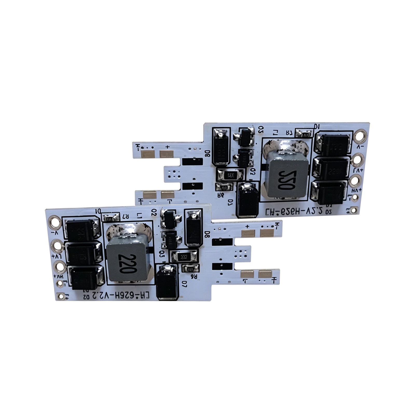
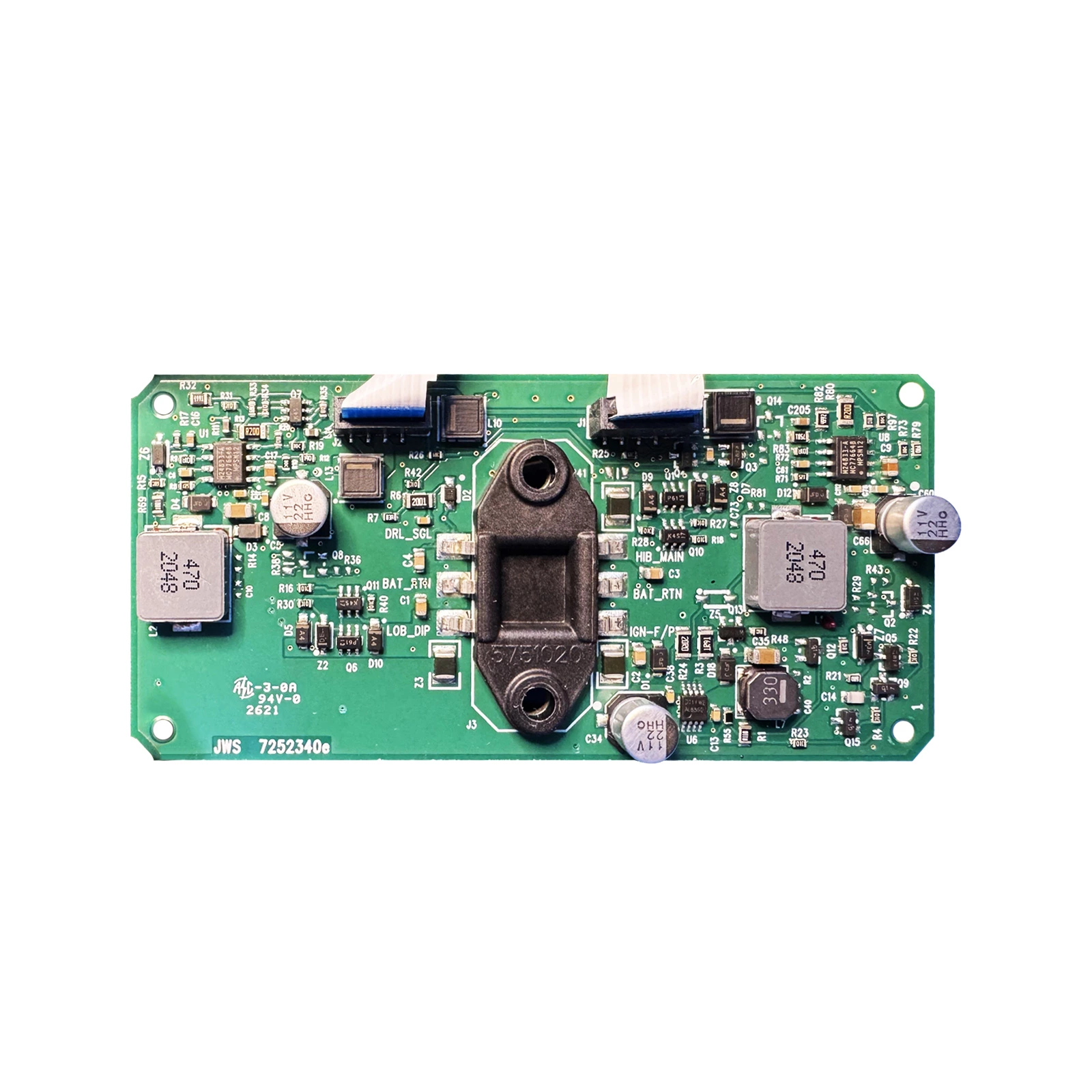
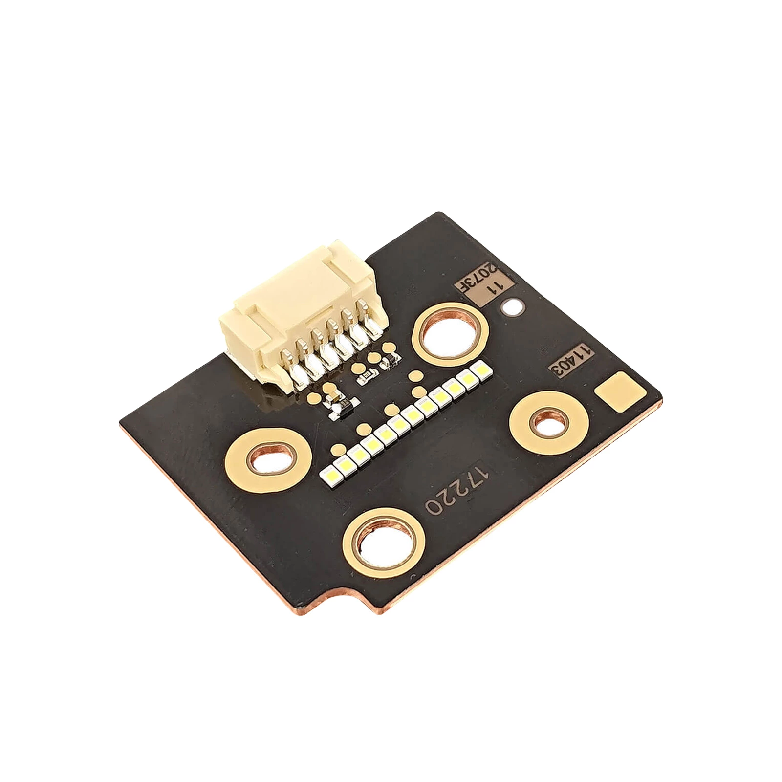
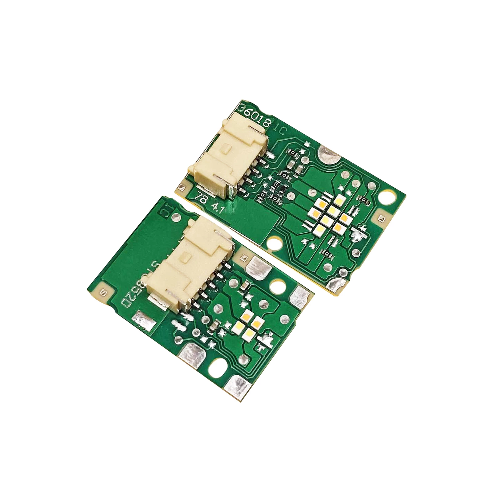
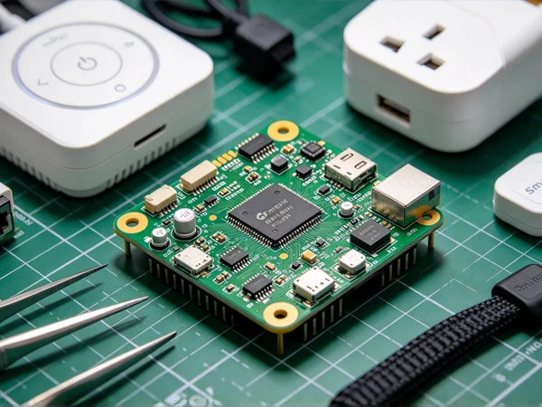
A smart home PCBA module is an assembled circuit board that provides one or more electronic functions within a connected home product. Depending on the application, it may include a microcontroller or system-on-chip (SoC), power management circuitry, sensors, communication components, memory, connectors, and supporting passive components.
A PCBA is different from a bare PCB. The bare PCB provides the conductive tracks and mounting structure, while the PCBA includes the electronic components assembled onto the board.
Common smart home applications include:
- Smart lighting: Lighting controllers, dimmers, and connected switches.
- Smart plugs and energy monitors: Power switching, current measurement, and energy monitoring.
- Smart locks and access systems: Control electronics, wireless connectivity, and user-interface interfaces.
- Environmental sensors: Temperature, humidity, motion, and other sensor-based functions.
- Smart thermostats: Control electronics, sensing interfaces, and connectivity.
- Home gateways and hubs: Communication and coordination between connected devices.
- Connected appliances: Control boards that integrate connectivity with appliance functions.
Each application has different requirements for component selection, PCB dimensions, power consumption, wireless performance, electrical safety, and testing.
A manufacturing solution should therefore begin with the product specification rather than assuming that all smart home boards require the same components or processes.
2. Wireless Connectivity Options for Smart Home PCBA
Wireless connectivity is an important consideration in many smart home products. The appropriate protocol depends on the product's function, operating environment, power budget, communication range, and intended ecosystem.
Wi-Fi
Wi-Fi is commonly used in devices that need direct network connectivity or relatively high data throughput. Applications include connected cameras, home gateways, displays, and certain appliances.
For PCBA manufacturing, relevant considerations include the selected wireless chipset, PCB layout, antenna arrangement, power supply stability, and the device's thermal environment.
Bluetooth Low Energy (BLE)
Bluetooth Low Energy is designed for low-power wireless communication and is frequently used in sensors, locks, remotes, and device commissioning.
Manufacturing considerations include component placement, antenna implementation, power management, and any required functional or radio-frequency testing.
Zigbee
Zigbee is used in many low-power smart home networks, particularly lighting and sensor applications. It operates over IEEE 802.15.4-based networking technology and can support mesh communication.
The suitability of Zigbee depends on the product architecture and the customer's existing ecosystem requirements.
Thread
Thread is an IPv6-based, low-power mesh networking technology built on IEEE 802.15.4. It is used in connected devices that require IP-based communication within a compatible network architecture.
PCB layout, antenna implementation, power management, and coexistence with other radios should be considered during product development.
Matter
Matter is an application-layer connectivity standard developed by the Connectivity Standards Alliance to improve interoperability among compatible smart home devices.
Matter works over supported network technologies, including Wi-Fi and Thread, while Bluetooth Low Energy can be used during commissioning. Matter does not replace the need to select appropriate wireless hardware or comply with applicable radio regulations.
Not every smart home product needs Matter. The decision depends on the target market, intended platform compatibility, product functionality, and customer requirements.
For OEMs, connectivity requirements should be confirmed early because they can influence chipset selection, PCB layout, firmware integration, antenna design, testing, and certification planning.
3. Key Manufacturing Challenges for Smart Home PCBA
Smart home products vary considerably in size, complexity, and operating environment. Several manufacturing considerations are particularly important when designing and assembling compact connected devices.
3.1 Miniaturization and Component Density
Many smart home devices must fit into compact enclosures, including wall switches, smart plugs, sensors, and battery-powered products.
Smaller PCBs can require fine-pitch components, compact passive components, dense routing, and careful component placement. These requirements place greater emphasis on solder paste printing, stencil design, placement accuracy, and reflow process control.
The appropriate manufacturing process depends on the actual component packages and PCB design. A board using 0201 or 01005 passive components, for example, may require tighter process controls than a board using larger components.
Before production, the manufacturer should review:
- Component package sizes and pitches
- PCB dimensions and panelization
- Pad geometry and solder mask clearances
- Stencil design and solder paste requirements
- Placement accuracy requirements
- Inspection access and test-point availability
A design for manufacturability (DFM) review can identify potential assembly issues before tooling and production preparation are completed.
3.2 Wireless Performance and PCB Layout
Wireless performance depends on more than the selected communication chipset. Antenna design, ground-plane geometry, RF routing, nearby components, enclosure materials, and the final product installation can all influence performance.
For this reason, wireless requirements should be considered during PCB design rather than left until the end of production.
A manufacturing review may include checking whether component placement follows the approved design, whether antenna keepout areas are respected, and whether the PCB revision matches the approved manufacturing files.
However, PCB assembly alone does not guarantee wireless range or radio performance. These results depend on the complete design and should be verified using suitable product-level or module-level test methods.
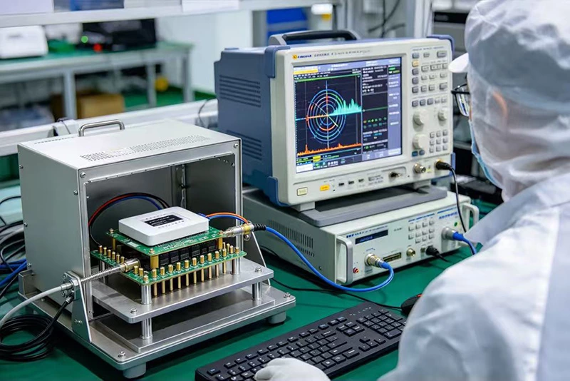
When RF performance is critical, the OEM and EMS partner should agree on the required tests, acceptance limits, test fixtures, and responsibility for radio validation.
3.3 Thermal Management and Power Stability
Smart home electronics may operate continuously or switch between different power states. Wireless transmission, processors, power converters, relays, and other components can generate heat depending on their design and operating conditions.
In compact enclosures, heat dissipation may be limited by PCB area, enclosure materials, airflow, and the proximity of heat-generating components.
Relevant design and manufacturing considerations include:
- Following component thermal and electrical specifications
- Maintaining the approved PCB stack-up and copper design
- Checking solder joint quality and component placement
- Verifying power supply behavior under specified operating conditions
- Evaluating thermal performance when required by the product specification
Thermal requirements should be validated for the intended product and enclosure. A manufacturing supplier should not infer long-term reliability from assembly inspection alone.
3.4 Power and Electrical Safety
Smart home products can operate at extra-low voltage, battery voltage, or mains voltage. The applicable electrical safety requirements depend on the product type, market, design, and intended use.
For products connected directly to mains power, PCB design and assembly may need to account for insulation, creepage and clearance distances, component ratings, protection circuits, and other applicable requirements.
These requirements should be reviewed during design and manufacturing preparation. A PCBA manufacturer should work to the approved drawings, BOM, and acceptance criteria, while product-level compliance remains dependent on the complete product and its applicable assessment process.
4. The Smart Home PCBA Manufacturing Process
A controlled manufacturing process helps maintain consistency between prototype builds and volume production. The exact workflow varies with the product design and customer requirements, but common stages include the following.
Stage 1: Design Review and Manufacturing Preparation
Before assembly begins, the manufacturing package should be reviewed for completeness and consistency.
Typical items include:
- Gerber or other approved PCB manufacturing data
- Bill of materials (BOM)
- Pick-and-place files
- Assembly drawings
- Component polarity and orientation requirements
- Approved component alternatives, if applicable
- Inspection criteria and test requirements
DFM and assembly reviews can identify potential issues such as insufficient component spacing, difficult-to-inspect solder joints, missing test points, and conflicts between the PCB design and the production process.
Changes should be documented and approved before being introduced into production.
Stage 2: Solder Paste Printing
For SMT assembly, solder paste is deposited onto the PCB pads through a stencil. The paste volume and position affect the quality of the solder joints formed during reflow.
The process should be controlled according to the stencil design, component geometry, solder paste specification, and PCB requirements.
Solder paste inspection (SPI), where specified or used as part of the process-control plan, can help identify printing issues before components proceed through reflow.
The inspection method and coverage should be agreed according to product risk, process capability, and customer requirements rather than assumed to be identical for every board.
Stage 3: Component Placement
Pick-and-place equipment positions electronic components onto the solder-paste-coated PCB.
Placement accuracy, component orientation, feeder setup, nozzle selection, and the quality of incoming components all affect the result.
For compact smart home boards, fine-pitch packages and small passive components may require particular attention during process setup and inspection.
Production preparation should use the approved BOM and placement program. Any substitutions or design changes should follow the customer's approval process.
Stage 4: Reflow Soldering
During reflow, the PCB passes through a controlled heating profile that melts the solder paste and forms solder joints.
The appropriate profile depends on the solder paste, component specifications, PCB thermal characteristics, and assembly requirements.
A validated profile should be used to balance solder joint formation with the thermal limits of the components and PCB assembly. Profile changes should be assessed and documented where required.
Stage 5: Post-Reflow Inspection
After reflow, inspection checks whether the assembly meets the defined workmanship and quality criteria.
Automated optical inspection (AOI) can help identify visible defects such as component misalignment, missing components, polarity errors, and certain soldering defects.
Some hidden solder joints or package structures may require other inspection methods, such as X-ray, depending on the design and risk assessment.
The applicable acceptance criteria should be agreed with the customer. Inspection results should be evaluated according to the product specification and the relevant workmanship standard, rather than assuming one inspection method can detect every defect.
Stage 6: Electrical and Functional Testing
The required test strategy depends on the product's function and the customer's quality requirements.
Possible methods include:
- In-circuit testing (ICT): Checks selected electrical characteristics and components where suitable test access is available.
- Functional circuit testing (FCT): Verifies that the assembled electronics perform defined functions under specified test conditions.
- Programming and configuration: Loads approved firmware or configuration data when included in the manufacturing scope.
- Connectivity testing: Checks selected communication functions when the appropriate test setup and acceptance criteria are available.
- RF testing: Measures specified radio-frequency performance when required and supported by suitable equipment and procedures.
Not every smart home PCBA requires every test method. The test plan should be defined according to the product architecture, risk, customer requirements, and available test access.
For wireless devices, board-level electrical testing and radio-performance validation are different activities. Passing one does not automatically prove compliance with all radio regulations or platform requirements.
Stage 7: Final Inspection and Traceability
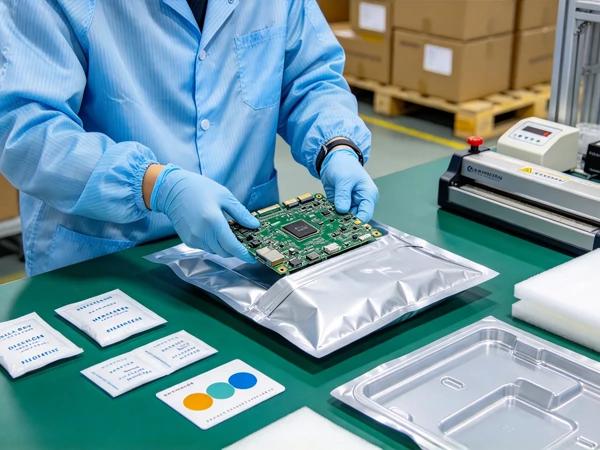
Before shipment, assemblies should be checked against the agreed release criteria. These may include visual inspection, test status, labeling, packaging, and required production documentation.
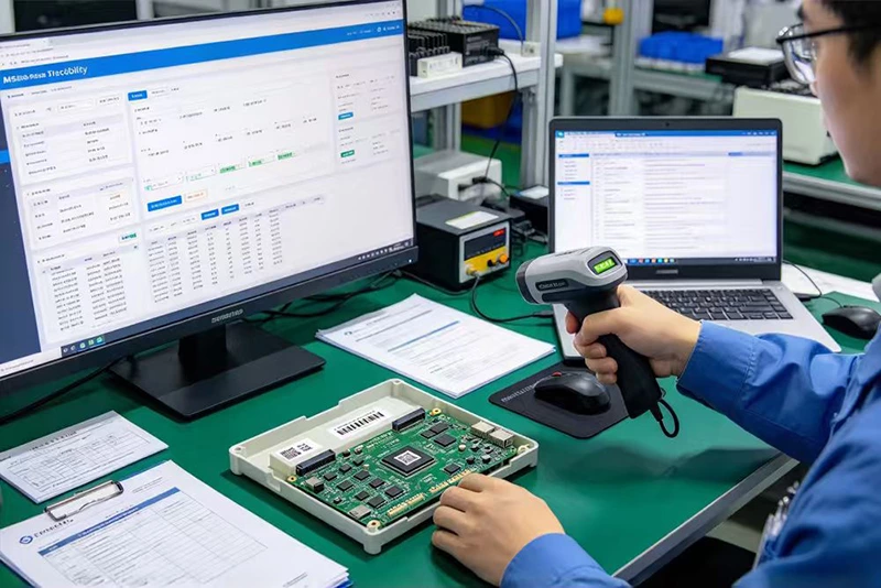
Traceability requirements vary by product and customer. Depending on the program, records may link the assembly to its PCB revision, component lots, production date, inspection results, and test records.
A documented traceability process can help manufacturers and customers investigate quality issues, identify affected production lots, and manage corrective actions more effectively.
5. Quality Control for Smart Home PCBA Manufacturing
Quality control should be designed around the product's failure risks and operating requirements. A single inspection step cannot verify every aspect of an electronic assembly.
An effective quality plan may include several complementary controls.
Incoming Material Control
Component quality and authenticity are important to assembly reliability. Incoming controls may include part-number verification, supplier documentation review, packaging inspection, lot identification, and other checks defined by the procurement and quality plan.
Critical components and approved substitutes should be managed according to the customer's BOM and approval requirements.
Process Control
Manufacturing controls should address the processes most likely to affect the product's quality, such as solder paste printing, component placement, reflow, and handling.
The specific controls may include setup verification, equipment maintenance, process parameter monitoring, and inspection at selected stages.
Workmanship Inspection
Assembly acceptance criteria should be defined before production. IPC-A-610 is one commonly referenced standard for assessing the acceptability of electronic assemblies, but the applicable revision and acceptance class should be agreed for the specific project.
The appropriate class depends on the product's intended use and customer requirements. It should not be assigned solely on the basis that a product is consumer electronics or smart home equipment.
Electrical and Functional Verification
Testing should address the functions that matter to the product. For example, a smart lighting controller may require checks of switching behavior and communication functions, while a sensor module may require verification of its sensor interface and power behavior.
The exact test coverage and pass/fail limits should be documented and approved.
Nonconformance and Corrective Action
When defects are identified, the response should include appropriate containment, investigation, and corrective action.
Defect trends can help identify recurring problems related to materials, assembly processes, design, or test coverage. Corrective actions should be verified to determine whether they address the underlying cause.
6. Regulatory and Certification Considerations
Smart home products sold in different markets may be subject to radio, electromagnetic compatibility, electrical safety, environmental, and other requirements.
The applicable obligations depend on the product, its intended use, the target market, and whether it incorporates pre-certified radio modules or other regulated components.
United States
Products with intentional radio transmitters may require authorization under applicable FCC rules. The relevant authorization pathway depends on the equipment and its configuration.
Using an approved radio module may simplify some aspects of product integration, but it does not automatically exempt the finished host product from every applicable requirement.
European Union
Radio-equipped products may fall under the Radio Equipment Directive (RED), depending on their design and intended use. Other legislation and standards may also apply.
CE marking represents the manufacturer's declaration that the product meets all applicable EU requirements; it is not a single universal certification that applies identically to every smart home PCBA.
Matter and Other Connectivity Programs
Matter certification addresses compliance with the Matter specification and interoperability within the applicable ecosystem. It is separate from regulatory radio authorization and other product safety obligations.
Other wireless technologies may have their own certification or qualification programs. The relevant requirements should be confirmed for the specific product and market.
How EMS Partners Can Help
An EMS partner may support manufacturing documentation, assembly quality, traceability, test implementation, and coordination with the customer's compliance team or external laboratories, depending on the agreed scope.
However, PCB assembly does not by itself establish that a finished smart home product is certified. OEMs should define responsibility for design validation, formal testing, certification applications, and final market compliance before production begins.
7. How to Choose an EMS Partner for Smart Home PCBA
Selecting an EMS partner requires more than comparing the quoted price per board. Buyers should determine whether the supplier's actual manufacturing capabilities and quality processes fit the product requirements.
7.1 Confirm Assembly Capabilities
Discuss the PCB dimensions, layer count, component packages, pitch requirements, assembly complexity, and expected volume.
Ask the supplier to explain how it assesses manufacturability and which requirements may need additional tooling, process validation, or specialist inspection.
7.2 Review Quality Controls
Ask how the supplier manages solder paste printing, placement, reflow, inspection, nonconforming products, and corrective action.
Where relevant, request examples of inspection records or quality reports from comparable programs, subject to confidentiality requirements.
7.3 Clarify Testing Responsibilities
Define which tests are included in the manufacturing quotation and which require additional equipment, fixtures, programming, external laboratories, or customer-supplied procedures.
For wireless products, clarify whether the supplier provides basic functional connectivity checks, calibrated RF measurements, or only assembly services. These capabilities are not interchangeable.
7.4 Evaluate Material and Supply Chain Management
Smart home products may depend on specific wireless SoCs, power management ICs, sensors, and other components with different availability and lifecycle risks.
Discuss BOM management, approved vendors, component traceability, change approval, and handling of obsolete or unavailable parts.
Alternative components should not be introduced without the required technical evaluation and customer approval.
7.5 Verify Production Capacity and Delivery Planning
Capacity claims should be evaluated in the context of the actual PCB design, component count, product mix, quality requirements, and delivery schedule.
Ask how the supplier estimates output, manages production changeovers, and plans material availability. A general placement-capacity figure is useful background information, but it is not a substitute for a project-specific capacity assessment.
7.6 Confirm Documentation and Traceability
Agree on which records will be retained and supplied, including relevant material records, inspection results, test data, product revisions, and lot information.
The required level of traceability should match the product's risk, the customer's quality system, and applicable contractual or regulatory requirements.
8. Working with TECOO on PCBA Manufacturing
TECOO provides electronics manufacturing services for customers developing and producing electronic products. For smart home projects, manufacturing requirements should be evaluated according to the product's PCB design, BOM, assembly complexity, quality specifications, and expected production volume.
TECOO operates 8 production lines with a monthly placement capacity of 82.368 million points per month . This figure describes component placement capacity, not the number of finished smart home PCBA modules produced each month. Actual project output depends on component count per board, production mix, process constraints, and other manufacturing requirements.
For a new smart home PCBA project, the initial manufacturing review should establish:
- The PCB design files and BOM
- The required assembly volume and delivery schedule
- Component package and placement requirements
- Inspection and functional testing requirements
- Any special wireless, electrical safety, or environmental constraints
- Packaging, labeling, and traceability requirements
These details help establish a realistic manufacturing plan and identify technical questions that need to be resolved before production.
If your team is developing a smart home controller, connected sensor, lighting board, gateway, or another electronic assembly, contact TECOO to discuss your PCBA manufacturing requirements and request a project-specific review.
Frequently Asked Questions
1. What is smart home PCBA manufacturing?
Smart home PCBA manufacturing is the process of assembling and verifying electronic circuit boards used in connected home products. It can include SMT assembly, inspection, programming, electrical testing, functional testing, and other services defined by the project.
2. Which wireless protocol is best for a smart home device?
There is no single best protocol for every product. Wi-Fi, Bluetooth Low Energy, Zigbee, Thread, and Matter serve different roles and requirements. Selection depends on power consumption, communication needs, product architecture, target ecosystem, and market requirements.
3. Does every smart home PCBA need Matter certification?
No. Matter is relevant to products designed to participate in the Matter ecosystem. Other smart home products may use different protocols or operate within other architectures. The requirements should be confirmed for the target product and market.
4. What tests are important for smart home PCBA?
Common tests include visual inspection, AOI, electrical testing, and functional testing. Depending on the product, additional methods such as X-ray inspection or RF measurements may be appropriate. The test plan should reflect the design, risk, customer requirements, and applicable standards.
5. Can an EMS supplier handle wireless certification?
An EMS supplier may support manufacturing documentation, test implementation, pre-compliance activities, or coordination with external laboratories, depending on its actual capabilities and the agreed scope. Formal certification responsibilities should be confirmed before the project begins.
6. How do I estimate production capacity for a smart home PCBA?
Start with the PCB design, component count, component mix, panelization, process requirements, and delivery schedule. The supplier should estimate project-specific throughput rather than relying solely on a general machine placement-speed figure.
7. What should I provide when requesting a PCBA manufacturing quotation?
Provide the BOM, PCB fabrication files, assembly drawings, expected volume, target delivery schedule, quality requirements, and any required inspection or testing procedures. Clearly identify special wireless, safety, programming, or traceability requirements so the supplier can assess the project accurately.
Conclusion
Smart home PCBA manufacturing requires coordination between product design, component selection, PCB assembly, testing, and quality management. Miniaturized components may require tighter assembly controls, wireless products need appropriate attention to RF design and validation, and regulatory obligations must be assessed according to the finished product and target market.
For OEMs and product developers, the right EMS partner is one that can explain its manufacturing capabilities, identify project-specific risks, implement agreed quality controls, and provide the documentation required for production and traceability.
By defining the product requirements early and validating the manufacturing process before scaling, companies can reduce avoidable production issues and build a more reliable path from prototype to volume manufacturing.
Planning a smart home PCBA project? Contact TECOO to discuss your assembly requirements, expected volume, and quality specifications.