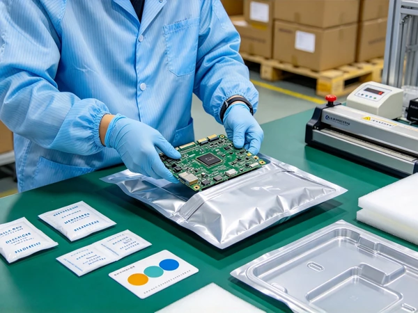
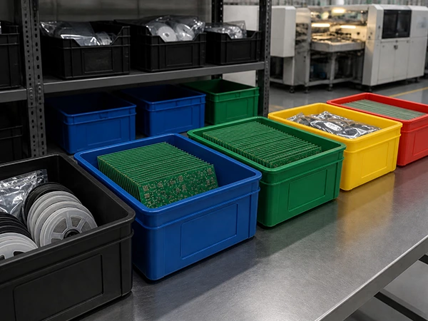
PCBA for Smart Home Automation System
[Core Answer] Smart home automation PCBA is defined by four simultaneous constraints: compact form factor, multi-protocol wireless capability, low standby power, and cost-effective high-volume assembly. Every design decision -- from wireless SoC selection to antenna placement to certification path -- flows from these constraints and must be resolved before tape-out, not after prototype failure.
6 Key Engineering Facts
- Smart home PCBA balance four simultaneous constraints: size, multi-protocol wireless, standby power, and high-volume assembly cost -- all of which must be addressed at design stage, not post-prototype.
- Matter -- the industry-unifying standard supported by Amazon, Apple, and Google -- operates over Wi-Fi and Thread, with Bluetooth LE for device commissioning. Targeting Matter compatibility affects wireless SoC selection and certification scope (CSA, csa-iot.org).
- Wireless protocol selection is the most consequential early design decision. Different protocols serve different device roles; mixing protocols on a hub PCBA has direct implications for antenna layout, RF isolation, and regulatory testing.
- FCC Part 15 authorization (US) and CE marking incorporating the Radio Equipment Directive (EU) are hard legal gates. Testing and authorization typically span 4-12 weeks per market; planning them after hardware finalization is a documented source of launch delays (WonderfulPCB, wonderfulpcb.com).
- FCC authorization for RF-enabled electronics typically costs $3,000-$5,000 and above, varying by protocol count and modulation complexity. US and EU authorizations are separate processes with separate documentation requirements.
- BGA solder joint quality at the wireless SoC is the primary manufacturing risk for smart home PCBA. X-ray inspection is the only practical method to verify joint formation; SPI before placement prevents the costlier outcome of discovering paste defects at functional test.
What Makes Smart Home Automation PCBA Different
Size pressure is constant. Consumer smart home devices are embedded in light switches, wall plugs, and door handles -- enclosures that leave little room for the electronics inside. A board that fits prototype form factor constraints easily may become too large when the industrial designer finalizes the housing. Working within a defined footprint from the earliest schematic stages is a requirement, not an option.
Power consumption determines product viability. Battery-powered devices (sensors, locks, remotes) live or fail by their standby power profile. A motion sensor drawing 50 uA in standby on two AA batteries achieves a multi-year battery life; the same sensor drawing 500 uA may need replacement every few months -- commercially unacceptable for a maintenance-free product. Every component must be evaluated for sleep-mode current draw alongside active-mode specifications.
Wireless connectivity is a functional requirement, not an add-on. Unlike industrial electronics where wired communication can be an option, smart home devices must connect wirelessly by design. The antenna, matching network, and RF front-end are first-class design elements. The antenna is typically one of the last things placed on a layout and one of the first things that causes certification failure if not positioned correctly.
Wireless Protocol Selection: The Foundation of PCBA Architecture
No single wireless protocol suits every smart home application. Protocol selection determines the RF silicon on the BOM, antenna configuration, network topology, gateway requirements, and the certification path the device must follow. Making this decision late in the design process forces board-level changes.
| Protocol | Frequency | Range | Power Profile | Network Topology | Primary Use Case |
| Wi-Fi 6 (802.11ax) | 2.4 / 5 GHz | 30-100 m | Medium-High | Star (AP-connected) | Cameras, speakers, doorbells |
| Bluetooth LE 5.x | 2.4 GHz | 10-100 m | Very low | Mesh or star | Sensors, locks, remotes |
| Zigbee (802.15.4) | 2.4 GHz | 10-100 m | Low | Mesh | Lighting, sensors, plugs |
| Thread (802.15.4) | 2.4 GHz | 10-100 m | Low | IP-based mesh | Matter-compatible devices |
| Z-Wave | 800-900 MHz | 30-100 m | Low | Mesh | Locks, thermostats, legacy |
| Matter over Wi-Fi | 2.4 / 5 GHz | Same as Wi-Fi | Medium | Bridge via controller | Hub-connected appliances |
Matter and its PCBA implications. Matter is an IP-based interoperability standard developed by the Connectivity Standards Alliance with backing from Amazon, Apple, Google, and dozens of manufacturers. Per CSA's published specification, Matter runs across Wi-Fi and Thread network layers, with Bluetooth LE serving as the commissioning channel for device onboarding (csa-iot.org). A Matter-compatible PCBA needs support for at least one of these transport layers, plus CSA-administered product certification and RF performance meeting the protocol's requirements across all supported bands.
Multi-protocol boards. Hub and gateway PCBAs often need simultaneous support for multiple protocols -- Wi-Fi for cloud connectivity, Thread for local device networks, Zigbee for legacy device compatibility. Designing these boards requires careful attention to RF isolation between co-located radio circuits, antenna placement to minimize inter-radio interference, and filtering to prevent one transmitter from desensitizing an adjacent receiver.
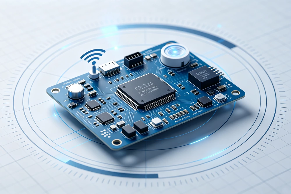
Key PCBA Design Considerations
Miniaturization and Component Density
Modern RF SoCs integrate MCU, wireless modem, and power management in a single QFN or BGA package -- reducing component count and board area simultaneously. Passives have migrated to 0201 and 01005 packages. The trade-off is assembly precision:
- Stencil apertures sized to deliver precise paste volumes at small pad dimensions
- Pick-and-place machines with vision systems capable of sub-100-um alignment tolerances
- Reflow profiles tuned for the board's specific thermal mass -- especially when large-mass connectors and small 0201 passives coexist
- AOI and X-ray inspection to verify solder joint quality under components where optical inspection provides no visibility
Antenna Design and Placement
The antenna is the component most likely to cause regulatory test failure in a smart home PCBA. Its position relative to ground planes, nearby metal structures, and the device enclosure directly determines radiated efficiency.
- Follow the wireless SoC manufacturer's reference antenna placement exactly. These placements are validated; deviations require re-characterization.
- Maintain the ground-free clearance zone around the antenna feed point as specified in the reference design.
- Validate antenna performance inside the final housing before committing to tooling. Free-space RF performance does not predict in-enclosure performance.
- For multi-band antennas (2.4 GHz + 5 GHz), use simulation tools to verify inter-antenna isolation before tape-out.
Power Management and Thermal Design
Battery-powered smart home PCBAs require careful power rail architecture: boost or buck converter to regulate the variable battery voltage, LDO for sensitive analog circuits, active power state sequencing for deep sleep between events, and current measurement infrastructure during development for state-by-state power profiling.
For mains-powered devices, thermal management is the relevant concern. Smart home wall plugs and dimmers must dissipate switching losses within a sealed plastic enclosure. The PCBA layout must provide adequate copper area for heat spreading, positioning high-dissipation components away from temperature-sensitive circuits and user-accessible areas.
Regulatory Certification Requirements
United States: FCC Part 15
Any wireless device sold in the United States requires FCC 47 CFR Part 15 authorization. For intentional radiators -- devices designed to transmit radio signals, which includes all wireless-enabled smart home PCBAs -- authorization involves laboratory testing of radiated emissions, conducted emissions, and for portable devices, SAR.
[Cost & Timeline] FCC authorization for RF-enabled electronics typically runs $3,000-$5,000 and above, varying with protocol count and modulation complexity. Standard processing spans 4-12 weeks from first submission (source: WonderfulPCB certification guide, wonderfulpcb.com). Using pre-certified wireless modules reduces authorization scope but requires SDoC and avoids configurations that void the module grant.
European Union: CE Marking
Radio Equipment Directive (RED, 2014/53/EU): Governs radio performance, interference, and cybersecurity for wireless devices sold in the EU.
RoHS Directive (2011/65/EU): Restricts ten hazardous substances across electronic equipment -- lead, mercury, cadmium, and specific flame retardants among them. All materials in the PCBA must comply. Lead-free solder (SAC alloys) is the standard manufacturing approach.
REACH Regulation: Controls substances of very high concern in the supply chain; relevant to PCB base materials and certain component coatings.
[Key Compliance Point] FCC and CE are separate, non-interchangeable authorizations. A device with US FCC authorization needs a completely separate CE marking process for EU market entry, with its own documentation, testing, and Declaration of Conformity. Planning both processes concurrently reduces total calendar time significantly.
Matter Certification
Devices targeting Matter compatibility must pass CSA-administered product certification, which verifies correct Matter specification implementation and multi-vendor interoperability. As the CSA describes the standard, Matter certification provides the assurance that devices across different brands function reliably together within a shared smart home environment (csa-iot.org). Hardware must meet the protocol's timing and RF performance requirements before the software stack can pass interoperability testing.
Manufacturing Considerations: Choosing the Right EMS Partner
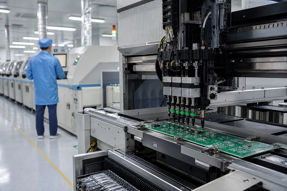
Smart home PCBA production requirements narrow the field of appropriate EMS partners. Fine-pitch assembly, RF-sensitive layouts, and power management circuits requiring precise solder joint quality rule out general-purpose contract manufacturers without consumer IoT experience.
SPI (Solder Paste Inspection) positioned immediately after the paste printer is essential for boards with 0201 passives and fine-pitch BGAs. Measuring paste volume and registration accuracy before any components are placed allows defective boards to be wiped and reprinted at zero component cost -- far less expensive than discovering the same defect at functional test.
X-ray inspection is required for BGA packages used in most RF SoCs. Joint formation quality -- solder ball height, void content, bridging -- is entirely invisible to optical methods. For wireless SoCs with 0.4 mm or 0.5 mm pitch BGAs, X-ray is the only practical pre-functional verification method.
Conformal coating may apply for devices installed in bathrooms, kitchens, garages, or outdoor enclosures. Selective automated dispensing achieves consistent protection without covering connector contacts or test points -- a precision that manual spray-and-mask processes cannot consistently replicate.
Questions to Ask a Prospective EMS Partner
- What is their demonstrated first-pass yield rate on consumer IoT boards with BGA counts comparable to your design?
- How are they managing solder paste -- temperature conditioning before use, working life tracking per opened container?
- Do they have in-house RF test capability or a validated relationship with a certified RF test laboratory?
- Can they provide component traceability to lot level for all active components?
- Does their DFM review process identify RF-related layout risks, or only component sourcing issues?
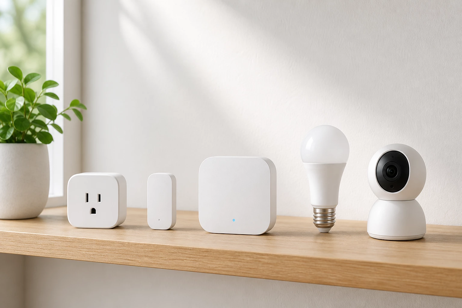
Application Scenarios by Device Type
| Device Type | Key PCBA Requirements | Wireless Stack | Form Factor |
| Smart sensor (door/motion/temp) | Ultra-low standby; coin cell/AA; small PCB | BLE 5.x or Zigbee | <30 x 20 mm |
| Smart lighting controller | Mains isolation; thermal mgmt; RFI suppression | Zigbee or Z-Wave | Fits wall box depth |
| Smart plug / outlet | Power metering IC; mains isolation; compact SMPS | Wi-Fi or Zigbee | Outlet housing |
| Smart lock | Security MCU; tamper detection; low-current wake | BLE + Z-Wave or Zigbee | Lock mechanism |
| Smart hub / gateway | Multi-protocol RF; higher processing demand | Wi-Fi + BLE + Thread or Zigbee | Desktop/wall-mount |
| Smart camera | Video ISP; high bandwidth; thermal management | Wi-Fi 6 or Ethernet | Module-based common |
FAQ
What is a smart home automation PCBA?
A smart home automation PCBA is an assembled circuit board that provides the core electronics for a connected home device -- sensor interface, wireless communication, power management, and control logic. It translates physical inputs (temperature, motion, switch state) into digital signals transmitted wirelessly to a home network and cloud platform. The PCBA determines wireless compatibility, battery life, and long-term reliability.
What wireless protocols should a smart home PCBA support?
Protocol selection depends on device type and target ecosystem. Battery-powered sensors and locks typically use Bluetooth LE, Zigbee, or Thread for low power consumption. Bandwidth-intensive devices use Wi-Fi. Hub devices often integrate multiple protocols simultaneously. For broad ecosystem compatibility, Matter -- which runs over Wi-Fi and Thread with BLE for commissioning -- is the emerging interoperability standard supported by major ecosystems (CSA, csa-iot.org).
What certifications does a smart home PCBA need?
At minimum: FCC Part 15 authorization for US sales; CE marking incorporating the Radio Equipment Directive and RoHS for EU sales. Devices targeting Matter compatibility additionally need CSA Matter product certification. Protocol-specific certifications (Wi-Fi Alliance, Bluetooth SIG) may also apply. US and EU markets each require separate, independent processes.
How long does FCC and CE certification take?
For standard wireless consumer electronics, each authorization process typically spans 4-12 weeks from initial submission. FCC authorization for RF-enabled products typically ranges from $3,000-$5,000 and above depending on protocol complexity (WonderfulPCB, wonderfulpcb.com). Running both processes simultaneously using shared pre-compliance test results reduces total calendar time where test overlap permits.
What assembly quality standards apply to smart home PCBA?
IPC-A-610 Class 2 is the baseline acceptability standard for consumer smart home PCBA, covering solder joint criteria, component placement tolerances, and cleanliness requirements. For devices with safety-related functions (smoke detectors, locks, leak sensors), Class 3 criteria may be appropriate for specific high-reliability joints. Discuss quality class requirements with your EMS partner during quotation.
Why does antenna placement matter so much in smart home PCBA?
The antenna's position relative to ground planes, metal components, and the device enclosure directly determines radiated efficiency. Poor placement -- too close to ground pours, behind metal shields, obscured by the enclosure -- reduces radiated power below FCC and CE minimum thresholds, causing regulatory test failure even when the radio circuit is correctly designed. Validating antenna performance inside the final housing before tooling commitment is one of the most cost-effective steps in connected device development.
What should I look for in an EMS partner for smart home PCBA?
Demonstrated experience with consumer IoT boards at comparable component densities; SPI as a standard inline process step (not optional); X-ray capability for BGA inspection; documented solder paste management procedures; and RF test support or validated third-party lab relationships. An EMS partner who reviews your design for RF-related DFM issues before quoting is providing the engineering engagement that reduces certification iteration risk.
References
1. Connectivity Standards Alliance (CSA) -- Matter Protocol Overview: csa-iot.org/all-solutions/matter/
2. WonderfulPCB -- Consumer Electronics Certification Requirements in the US and EU: wonderfulpcb.com
3. SprintPCB Group -- Industrial IoT PCB Assembly: Design and Manufacturing Considerations: sprintpcbgroup.com
4. IPC-A-610 -- Acceptability of Electronic Assemblies: electronics.org/ipc-a-610
5. EU RoHS Directive 2011/65/EU: European Commission RoHS