Charging Device PCBA: GaN Power Stages, USB PD 3.1 & Safety Certification Requirements
Key Takeaways
1. Charging device PCBA is among the highest-volume, highest-regulatory-scrutiny segments in consumer electronics manufacturing — a single thermal runaway event caused by a non-compliant power conversion board can trigger a product recall affecting hundreds of thousands of units and permanently damage a brand's market position.
2. Consumer electronics PCBA for charging applications must satisfy a multi-standard certification stack simultaneously: UL 62368-1 for North America, IEC 62368-1 for global/EU, PSB for Singapore, PSE for Japan, and KC for South Korea — each with distinct isolation requirements, creepage/clearance distances, and thermal performance criteria.
3. GaN (Gallium Nitride) power stage integration is now the primary technical differentiator in premium charging device PCBA, enabling power densities of 1–2 W/mm² at switching frequencies above 1 MHz a specification that demands PCB stackup, component placement, and thermal management discipline that standard low-frequency PCBA production processes cannot deliver.
4. USB Power Delivery 3.1 protocol compliance requires charging PCBA to support programmable power supply (PPS) output up to 48V / 5A with ±5% voltage accuracy at every PD negotiated voltage step — a precision requirement that cascades into ADC selection, feedback loop design, and component temperature coefficient specifications across the entire power conversion chain.
5. Overseas brand owners sourcing charging device PCBA from Chinese manufacturers report an average certification-stage failure rate of 23% on first-submission products where the manufacturer was not engaged in DFM review for certification compliance — a preventable failure mode that adds 8–16 weeks and $15,000–60,000 in retesting and redesign cost per product.
Core Definition Opening
Charging device PCBA sits at the intersection of power electronics, RF engineering, and consumer safety regulation. Most PCBA factories can build one of those three. Few can build all three.
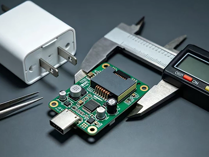
A USB-C GaN charger looks simple. It is a box roughly 40mm × 40mm × 25mm with a wall plug on one side and a USB-C port on the other. The assembled PCB inside that box contains a GaN FET switching at 1–2 MHz, a flyback or LLC resonant power conversion topology, a USB Power Delivery controller managing real-time voltage and current negotiation with the connected device, thermal protection circuitry, primary-to-secondary isolation with >4,000V surge withstand, and regulatory-compliant creepage and clearance distances that must be maintained across temperature extremes and humidity cycling.
That is not a simple board. It is a precision power electronics assembly operating under regulatory requirements that evolved specifically because inadequate designs cause fires, electric shock, and battery damage.
Consumer electronics PCBA for charging devices covers a product family wider than wall chargers alone: wireless charging transmitter and receiver boards, power bank assemblies with multi-cell battery management, automotive-grade in-vehicle charging modules, desktop charging stations managing multi-port PD negotiation, and industrial-adjacent USB-C docking stations with integrated power delivery. Each application shares the core power conversion challenge but differs in form factor, certification pathway, and production volume requirements.
This guide is written for consumer electronics brand owners, hardware developers, and procurement managers who specify and source charging device PCBA. It covers the technical requirements that separate compliant from non-compliant designs, the certification landscape, the production standards that ensure consistency, and the supplier selection criteria that determine whether your charging product reaches market safely and on schedule.
Unique Technical Requirements of Charging Device PCBA
Power Conversion Topology and Switching Performance
The power conversion topology determines the PCB's switching frequency, magnetic component requirements, and EMI profile. Three topologies dominate charging device PCBA:
Flyback topology is the workhorse of single-output chargers below 65W. It provides galvanic isolation between input (mains AC) and output (DC charging rail) through a transformer, operates efficiently across the wide input voltage range (85–265V AC) required for global market products, and is manufacturable with standard SMT processes. The limitation: switching frequency is typically limited to 65–130 kHz with silicon MOSFETs, producing a transformer that occupies 30–40% of PCB area in a compact charger.
LLC resonant topology extends efficiency and enables higher switching frequencies (130–500 kHz) by operating the power conversion stage at resonance, reducing switching losses. It is the standard topology for chargers above 45W where efficiency regulation (EU Ecodesign Directive, US DOE Level VI) penalizes designs with standby losses above 75mW. LLC topology requires tighter magnetic component tolerances and more complex feedback control — PCB requirements include controlled impedance on the resonant tank components and higher attention to parasitic inductance at the GaN or SiC switching nodes.
GaN-based active clamp flyback or LLC enables switching frequencies above 1 MHz with GaN FETs, compressing transformer size by 60–70% compared to silicon-based designs at equivalent power levels. A 65W GaN charger can achieve a volume of 32–45 cm³ versus 80–120 cm³ for a silicon-based equivalent. The PCB manufacturing requirements for GaN-based charging PCBA are fundamentally different: switching node copper area must be minimized to reduce parasitic capacitance, gate driver layout must be optimized for nanosecond-scale switching transitions, thermal pad design for bare-die GaN packages requires tighter solder paste stencil aperture control than standard IC packages, and the PCB laminate must maintain stable dielectric properties at 1 MHz+ operating frequencies.
USB Power Delivery and Protocol Compliance
USB Power Delivery 3.1 is the current standard for high-power device charging, supporting negotiated output voltages of 5V, 9V, 15V, 20V, 28V, 36V, and 48V, and output currents up to 5A. The PD controller IC manages this negotiation over the CC (Configuration Channel) pins of the USB-C connector via the BMC (Biphase Mark Coding) communication protocol.
From a PCBA perspective, PD protocol compliance imposes: voltage regulation accuracy of ±5% at every negotiated voltage step; current limiting response time below 100ms for overcurrent events; CC line ESD protection rated to IEC 61000-4-2 Level 4 (±8kV contact discharge) without compromising CC signal integrity; and a power path switching architecture that transitions between negotiated voltage levels without dropout events that reset or damage the connected device.
Programmable Power Supply (PPS) mode — the sub-protocol that enables fast charging algorithms on Samsung, Xiaomi, OPPO, and Apple devices — adds variable voltage output in 20mV steps and current limit in 50mA steps. PPS requires a higher-bandwidth feedback loop and more precise voltage reference than fixed-voltage PD output — specification requirements that cascade into component selection across the entire power conversion chain.
Wireless Charging and Qi / MagSafe Integration
Wireless charging transmitter PCBA operates on resonant inductive coupling at 100–205 kHz (Qi standard) or higher frequencies for proprietary fast wireless protocols. The transmitter coil is either a separate ferrite-backed coil assembly or a multi-coil array (for spatial freedom charging) whose PCB-mounted driver electronics generate the alternating current at the required frequency and power level.
Qi 2.0 certification (released 2023) and Apple MagSafe compatibility impose alignment detection, foreign object detection (FOD), and power transfer efficiency requirements that are validated at the system level — transmitter PCB and coil together — not independently. PCBA manufacturing for wireless charging transmitters must maintain coil-to-driver impedance matching specifications across production tolerances, which requires controlled inductance values in the PCB trace forming the resonant tank.
Thermal Management at High Power Density
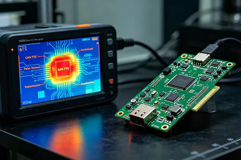
A 140W USB-C GaN charger operating at 92% conversion efficiency dissipates approximately 12W as heat within a volume of approximately 60–80 cm³. That heat must be conducted from the GaN die through the PCB thermal via array, through any thermal interface material, to the enclosure surface — without any component temperature exceeding its rated maximum.
Thermal management in charging device PCBA is a PCB layout problem, not just a component selection problem. GaN FET thermal pads require: minimum thermal via diameter of 0.3mm, maximum thermal via pitch of 0.6mm, and filled/capped vias to prevent solder wicking into the via holes during reflow. Copper pour on internal layers below the GaN device extends the thermal spreading area. The thermal resistance from junction to case (θjc) of the GaN device, combined with the PCB thermal via resistance and the thermal interface material resistance, determines whether the device stays within its rated operating junction temperature — a calculation that must be verified during DFM review, not discovered during product reliability testing.
Why Standard Consumer PCBA Processes Cannot Meet Charging Device Requirements
Creepage and clearance distance control. Safety-certified charging PCBA requires minimum creepage (surface distance between conductors) and clearance (air gap between conductors) distances between primary (mains-referenced) and secondary (output-referenced) circuits. For a working voltage of 265V AC with basic insulation, IEC 62368-1 requires a minimum creepage distance of approximately 6.4mm for Pollution Degree 2 environments. This is a hard physical constraint on PCB layout — it cannot be verified by functional testing and must be implemented correctly during PCB design and verified during production inspection. A standard PCBA factory without specific safety PCB layout experience will not automatically flag creepage violations during DFM review.
High-voltage primary circuit handling. The primary side of an isolated AC-DC converter operates at rectified mains voltage (up to 375V DC for 265V AC input). This requires: minimum PCB creepage and clearance to secondary circuits, X and Y safety capacitors with AEC-Q200-grade voltage ratings and failure mode qualification (X capacitors must fail open, Y capacitors must fail open or short with defined energy limits), and primary-side circuit handling procedures during assembly and testing that require trained operators and appropriate safety isolation procedures. Standard consumer PCBA factories trained on 5V logic board assembly are not automatically equipped for high-voltage primary-side assembly.
Isolation transformer winding and placement. The isolation transformer — the component that provides galvanic isolation between mains and output — must be placed with adequate clearance to all primary and secondary circuit elements on the PCB. The transformer windings themselves must maintain defined layer-to-layer insulation voltage withstand (typically >3,000V AC for 1 minute per IEC 62368-1). This is a component specification requirement, not a PCB requirement, but the PCBA factory must verify transformer compliance documentation (winding insulation test reports from the transformer manufacturer) before use in production.
EMI compliance at 1 MHz+ switching frequencies. GaN-based chargers switching at 1–2 MHz generate conducted and radiated EMI in frequency bands that are more difficult to filter than lower-frequency silicon-based designs. The filter design — X/Y capacitor selection, common-mode choke inductance value, and physical placement on the PCB relative to the switching node — must be validated against CISPR 32 (radiated) and CISPR 14-1 (conducted) limits before certification testing. Standard consumer PCBA factories without EMC pre-compliance testing capability cannot support this validation step.
Core Composition of Qualified Charging Device PCBA
Power Stage
GaN or silicon MOSFET with gate driver IC, bootstrap capacitor, snubber network (for flyback topology: RCD or active clamp), resonant tank components (for LLC: resonant inductor and resonant capacitor with defined Q factor), and primary-side current sensing. GaN bare-die packages require specialized solder paste stencil with 100μm aperture tolerance — standard stencil manufacturing tolerances of ±25μm are insufficient.
Isolation and Magnetics
Isolation transformer with UL/IEC-certified winding insulation, optocoupler or primary-side regulation IC for feedback across the isolation barrier, and isolation capacitors where applicable. Transformer placement must maintain PCB creepage distance from primary-side circuit traces.
Output Power Management
Synchronous rectification MOSFETs, output filter inductors and capacitors (low-ESR, rated to the output voltage and ripple current requirements), and output voltage and current sensing resistors with ±0.1% tolerance for PD voltage accuracy.
PD/Protocol Controller
USB Power Delivery controller IC managing CC communication, power negotiation state machine, and output voltage/current commands to the PWM controller. Supporting components: CC line ESD protection diodes, CC line filter capacitors, and VBUS overvoltage protection.
Safety and Protection
Input overvoltage protection, output overvoltage and overcurrent protection with response time below 100ms, thermal shutdown with automatic restart, surge protection (IEC 61000-4-5 Level 3 or Level 4 for commercial or industrial applications), and input inrush current limiting (NTC thermistor or active inrush control).
EMI Filter
Input EMI filter: common-mode choke, X capacitor (line-to-line), Y capacitors (line-to-earth, safety class Y1 or Y2 depending on application), and input rectifier bridge. Placed as close to the AC input as physically possible with minimal PCB trace length between filter components.
Thermal Management
GaN thermal pad with filled/capped via array, copper pour on internal layers below power components, and thermal interface pad or direct contact to enclosure metal for heat conduction to the outer surface.
Comparison Table: Standard Consumer PCBA vs Charging Device PCBA
| Specification | Standard Consumer PCBA | Charging Device PCBA | Design Impact |
| Operating voltage | 1.8V–5V (logic level) | 85–375V DC (primary), 5–48V (output) | Safety isolation, creepage/clearance design |
| Switching frequency | N/A (digital logic) | 65 kHz–2 MHz | PCB laminate selection, EMI filter design |
| PCB laminate | Standard FR4 (Tg 130°C) | High-Tg FR4 (170°C+), Rogers for GaN | Thermal stability, dielectric performance at frequency |
| Surface finish | HASL (standard) | ENIG (mandatory for fine-pitch GaN pads) | Solder joint quality on GaN bare-die pads |
| Creepage/clearance | Not applicable | 6.4–8mm primary-to-secondary minimum | PCB layout constraint, verified at inspection |
| EMC standard | IEC 61000-4-2 Level 2 | CISPR 32 / CISPR 14-1 + IEC 61000-4-5 Level 3 | EMI filter design, board layout shielding |
| Certification required | CE marking (basic) | UL 62368-1, IEC 62368-1, PSE, KC, PSB | Pre-compliance testing, design documentation |
| Thermal via density | Standard (functional only) | High-density filled vias under GaN (0.3mm pitch) | Stencil aperture tolerance, via fill process |
| Inspection standard | IPC-A-610 Class 2 | IPC-A-610 Class 2 with safety-critical Class 3 zones | Isolation spacing inspection, high-voltage zone handling |
| Component sourcing | Standard distributor | Safety-rated components only (UL/IEC recognized) | Y capacitors, X capacitors, optocouplers — certified parts |
| Production test | Functional test | Hi-Pot isolation test (3,000V AC / 1 min) mandatory | Requires dedicated Hi-Pot test equipment and trained operators |
| Typical cost premium vs. logic PCB | Baseline | +35–60% | Power components, safety parts, certification-grade process |
Main Application Scenarios for Charging Device PCBA
GaN Wall Chargers (20W–240W)
The fastest-growing segment in consumer charging hardware, driven by GaN technology enabling compact multi-port chargers that replace multiple device-specific adapters. PCBA requirements: bare-die GaN package assembly with high-density thermal via array, PD 3.1 multi-port power sharing logic (one 100W output that de-rates to 65W+45W when both ports are active), and CISPR 32 Class B EMI compliance for residential environments. Volume range: 5,000–500,000 units per model for established brands.
Wireless Charging Pads and Stands (5W–50W)
Qi 2.0 and proprietary fast wireless charging (Xiaomi 80W, OPPO 50W AirVOOC, Apple MagSafe 15W) transmitter boards require foreign object detection (FOD) sensitivity below 150mg metallic object mass, alignment detection for MagSafe-compatible positioning, and coil driver efficiency above 75% at rated power to meet Qi 2.0 efficiency requirements. The transmitter coil assembly — ferrite sheet, coil winding, and NTC temperature sensor — integrates with the PCBA as a sub-assembly that must be tested as a system.
Power Banks (5,000–30,000 mAh)
Power bank PCBA integrates battery management (multi-cell lithium polymer or cylindrical cell balancing, charging, and protection), boost conversion (3.7V battery to 5V/9V/15V/20V USB output), PD protocol controller, and pass-through charging (simultaneous input and output). The PCB must handle bidirectional power flow — charging in from a wall adapter while simultaneously discharging to a connected device — with appropriate power path management to prevent overloading the battery cells.
Automotive USB Charging Modules
In-vehicle USB charging ports (OEM instrument panel or aftermarket) must meet AEC-Q100 component qualification, operate over -40°C to +85°C (extended to +105°C for engine compartment locations), survive 14.4V nominal with 40V load dump transients, and comply with CISPR 25 (automotive EMC) for conducted and radiated emissions. Consumer electronics PCBA processes are not qualified for automotive applications without specific component substitution and process validation.
Desktop Multi-Port Charging Stations
6–12 port charging stations managing 200–300W total output require power distribution PCBs with per-port PD negotiation, current sharing between ports, overtemperature protection linked to a thermal management system (fan control or thermal throttling), and enclosure-integrated LED status indication per port. The power distribution PCB is distinct from the main power conversion PCB — a two-board architecture common in high-power desktop stations that simplifies certification and service replacement.
Laptop GaN Chargers (65W–240W)
High-wattage laptop chargers face the most demanding combination of size constraints, efficiency requirements, and EMI compliance obligations. EU Ecodesign Regulation (EU) 2019/1782 mandates no-load power consumption below 75mW and active mode efficiency above 87% at 50% load — requirements that require LLC or active clamp flyback topology with GaN power stages. The PCB must fit within an enclosure typically smaller than 60cm³ for a 100W product, requiring multilayer board design (4–6 layers) with precision power stage layout.
Standard Production Flow for Charging Device PCBA Orders
Stage 1: Safety-Focused DFM Review (Days 0–4)
DFM review for charging PCBA extends beyond standard SMT manufacturability checks. It must include: creepage and clearance verification against the target certification standard (IEC 62368-1 for EU/global, UL 62368-1 for North America), isolation barrier component placement review, GaN thermal pad and via design analysis, EMI filter component placement optimization for maximum common-mode rejection, and Hi-Pot test clearance (the test probes must access primary-side circuit without bridging across the isolation barrier). A DFM report that does not address these safety-specific items is a consumer-grade DFM applied to a safety-critical product.
Stage 2: Safety Component Verification (Days 1–5, parallel)
Every safety-critical component must be verified against the target certification standard before BOM lock: Y capacitors must carry UL/IEC recognized component status (Y1 or Y2 class as required); X capacitors must be AEC-Q200 qualified or UL/IEC recognized; optocouplers must carry CTR (current transfer ratio) and isolation voltage ratings matching the design requirement; the isolation transformer must have insulation test documentation from the transformer manufacturer; and GaN devices must be from the authorized supply chain, not grey-market or spot-market sources.
Stage 3: PCB Fabrication with Safety Specifications (Days 3–8)
High-Tg FR4 or Rogers laminate for GaN designs. IPC Class 3 fabrication quality for isolation barrier zones. Controlled impedance on switching node traces. Via fill and cap for GaN thermal pad vias. Minimum slot clearance for creepage enforcement between primary and secondary copper. Fabrication inspection must verify clearance distances as-fabricated, not just as-designed.
Stage 4: SMT Assembly — Safety Zone Protocols (Days 8–12)
High-voltage primary circuit assembly requires operator training and process controls beyond standard consumer SMT: solder paste volume for GaN bare-die pads verified by SPI before placement; X-ray inspection mandatory for GaN package solder joint verification; isolation transformer placement verified for creepage clearance to adjacent copper features; and AOI calibrated for safety-critical zone inspection criteria.
Stage 5: Hi-Pot Isolation Testing (Days 12–13)
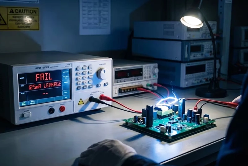
Every assembled unit undergoes Hi-Pot (High Potential) dielectric withstand testing: 3,000V AC applied across the primary-to-secondary isolation barrier for 1 minute (IEC 62368-1 minimum), or higher voltages for specific certification requirements. Hi-Pot testing requires dedicated equipment, trained operators with appropriate safety PPE, and a documented test procedure with pass/fail criteria. A factory that does not perform Hi-Pot testing on 100% of charging PCBA units is shipping product with undetected isolation failures.
Stage 6: Functional Testing and Protocol Validation (Days 13–15)
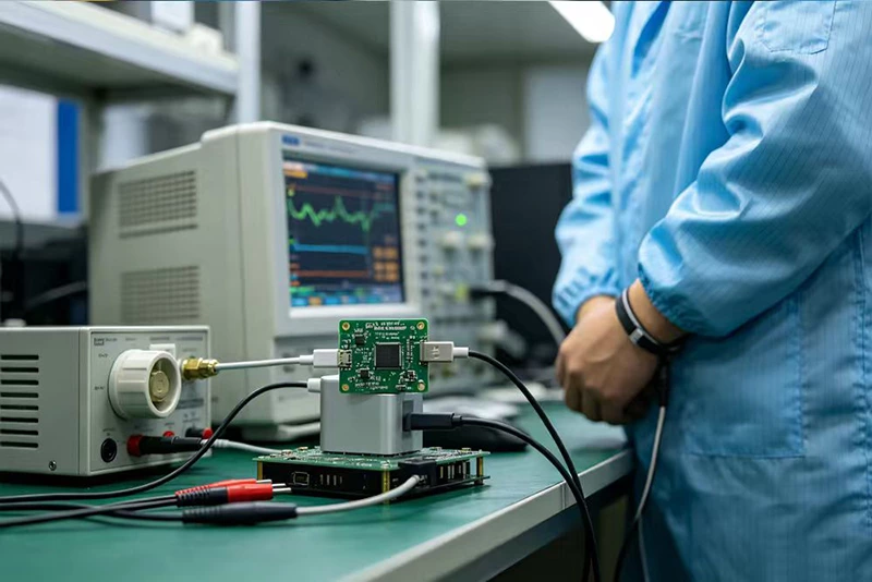
Full USB PD protocol compliance testing with a PD analyzer (Ellisys, LeCroy or equivalent): verify all advertised voltage/current combinations, PPS step resolution, PD communication timing, and overpower protection response. For wireless charging boards: Qi protocol compliance testing with standard receiver device and power transfer efficiency measurement. Output voltage accuracy at each PD negotiated level: ±5% maximum per USB PD 3.1 specification.
Stage 7: Burn-In and Thermal Validation (Days 15–18)
Powered burn-in at rated output load, 40–70°C ambient temperature, for 24–48 hours. Thermal imaging of the assembled board at rated load to confirm all component temperatures remain within rated maximums and to identify any thermal hotspots introduced by production process variation (insufficient solder on GaN thermal pad, poor thermal contact between component and PCB copper).
Stage 8: Pre-Shipment Inspection and Certification Documentation (Days 18–20)
Final electrical safety compliance check (leakage current measurement per IEC 62368-1 Annex P, touch current <0.5mA). Certification marking verification (correct CE mark, UL listing mark, or other regional marks as applicable). Documentation package: Hi-Pot test records by unit serial number, functional test results, burn-in records, and component lot traceability.
Key Production Standards and Certifications Required
IEC 62368-1 (Edition 3) — the unified audio/video, information technology, and communications technology safety standard, replacing IEC 60950-1. Mandatory for EU market access (CE marking under LVD Directive 2014/35/EU) and adopted as the reference standard in most global markets. Specific to charging devices: isolation requirements, creepage/clearance distances, transformer insulation, and Hi-Pot test voltages.
UL 62368-1 — the US/Canadian version of IEC 62368-1, administered by UL Solutions. Required for products sold through North American retail channels and carried by major US distributors. UL listing requires manufacturing inspection by UL at the production facility — not just product testing — meaning the PCBA factory must be prepared for periodic UL factory audits.
FCC Part 15 Subpart B — US mandatory emission standard for any digital electronic device, including chargers with switching power supplies. Conducted emissions to CISPR 14-1 limits and radiated emissions to FCC limits. First-submission failure rate for GaN chargers is high due to EMI generated at 1 MHz+ switching frequencies — pre-compliance testing before formal FCC submission is strongly recommended.
CISPR 32 / EN 55032 — EU radiated and conducted emission limits for multimedia equipment, applicable to charging devices. Class B limits (residential) are more stringent than Class A (industrial). A GaN charger that passes CISPR 32 Class B limits at all harmonics of its switching frequency demonstrates robust EMI filter design.
PSE (Product Safety Electrical Appliance & Material, Japan) — mandatory for all electrical products sold in Japan. Chargers fall under the Electrical Appliance and Material Safety Act (DENAN), requiring PSE mark on the product. PSE testing is performed by registered testing laboratories (JET, TÜV Japan, etc.).
KC Mark (Korea Certification) — mandatory for electrical products imported into South Korea, administered by KTC (Korea Testing Laboratory) or other accredited bodies. KC testing for chargers includes safety, EMC, and energy efficiency evaluation.
PSB (Singapore) — Safety Mark certification required for chargers sold in Singapore, administered by the Consumer Protection (Safety Requirements) Registration Scheme under the Singapore Safety Authority.
USB-IF Certification (USB Power Delivery) — while not a regulatory requirement, USB-IF PD compliance certification is increasingly required by major retailers and platform distributors (Amazon, Best Buy, Apple authorized reseller program) as a condition of product listing. USB-IF certified products carry the Certified USB logo and are listed in the USB-IF compliance database.
Energy Efficiency Standards — EU Ecodesign Regulation (EU) 2019/1782, US DOE Level VI, and California's Title 20 standard impose minimum energy efficiency at 25%, 50%, 75%, and 100% rated load, and maximum no-load power consumption. Chargers that do not meet these efficiency tiers cannot be legally sold in the respective markets, making efficiency validation a pre-production design gate rather than a post-production certification step.
Common Pitfalls When Sourcing Charging Device PCBA
Selecting a supplier that performs Hi-Pot testing on samples only. Hi-Pot testing must be performed on 100% of units — this is both a best practice and an implicit requirement of IEC 62368-1 compliance. A factory that Hi-Pot tests 5 units per batch has tested 5 units. The other 4,995 have unverified isolation integrity. One isolation failure in a shipped product reaching a consumer is a safety incident. Accept nothing less than 100% Hi-Pot testing with per-unit test records.
Treating Y capacitor selection as interchangeable. Y capacitors connected across the isolation barrier carry mains voltage in the event of a primary circuit fault. Their failure mode is critical: Y capacitors must fail open (not short) to prevent a mains voltage path to the accessible output side. Y1 class capacitors are rated for 500V AC peak / 250V AC working and are required for double-insulated products. Y2 class are rated for 300V AC peak / 150V AC. Using Y2 capacitors where Y1 is required — or using non-safety-rated ceramic capacitors as Y capacitors — is a certification violation and a product liability exposure.
Underspecifying the GaN thermal pad via design. The most common GaN charging PCBA manufacturing failure mode is insufficient thermal conductivity through the PCB via array below the GaN die. Symptoms: charger operates normally at 20°C ambient but thermal shuts down at 35°C ambient under full load. Root cause: thermal vias were sized correctly by area but not correctly by fill quality — hollow vias have 40–60% lower thermal conductivity than filled/capped vias. Specify filled and capped thermal vias for GaN packages and verify fill quality by cross-section inspection on the first production batch.
Failing to validate EMI compliance before certification submission. GaN chargers are among the most EMI-challenging consumer electronics products due to high-frequency switching and compact board layout. An EMI pre-compliance test using a near-field probe and spectrum analyzer — performed at the PCBA factory or a partnered test lab before sending product to a certification laboratory — identifies emission problems and their physical location on the PCB before the $3,000–8,000 certification laboratory slot is consumed. First-submission failures without pre-compliance testing are a direct consequence of skipping this step.
Not specifying efficiency class in the purchase order. EU Ecodesign and US DOE Level VI have specific efficiency requirements that must be validated during production, not assumed from the reference design. A PCBA factory that builds to the schematic without verifying output efficiency will ship product that may fail regulatory efficiency testing in the destination market. Specify the efficiency standard, the measurement method (voltage/current at 25%, 50%, 75%, 100% load), and the pass/fail criteria in the production test specification.
Accepting component substitutions on safety-rated parts without re-evaluation. When a Y capacitor, X capacitor, optocoupler, or isolation transformer goes on allocation, the factory may propose an alternate. For standard components (MCUs, passive resistors, capacitors), the buyer's BOM alternate part number process handles this. For safety-rated components, the alternate must carry equivalent UL/IEC recognition — a different brand Y capacitor at the same capacitance value is not automatically equivalent if it carries a different safety rating class or voltage rating. Every safety-rated component substitution must be reviewed by the buyer's engineering team before production resumes.
How to Select Reliable Charging Device PCBA Suppliers
Mandatory qualification criteria:
- Active Hi-Pot test capability with 100% per-unit testing and digital test records per serial number — ask to see a Hi-Pot test record from a recent production batch
- IPC-A-610 Class 2 with documented safety-critical zone procedures for primary-side high-voltage assembly — request the work instructions for primary-side assembly and Hi-Pot test operators
- Safety component sourcing policy: Y and X capacitors, optocouplers, and isolation transformers sourced exclusively from UL/IEC recognized component manufacturers — verify by requesting a recent purchase record for Y capacitors including the UL recognition file number
- Active GaN package assembly experience: ask for the specific GaN FET packages assembled in recent production (GaN Systems GS-065-011-1-L, EPC eGaN FETs, or Navitas NV6115/NV6125 are common references) and the stencil aperture and via specifications used
- EMI pre-compliance testing capability or established partnership with a certified EMC test laboratory
Differentiation criteria for premium charging PCBA partners:
- In-house efficiency measurement capability (electronic load + precision power analyzer, not estimated from calculated losses)
- USB-IF PD compliance testing equipment or established USB-IF authorized laboratory partnership
- Wireless charging coil integration and Qi protocol testing capability for wireless charging product lines
- Documented experience with UL factory inspection process (UL listing for charger products requires periodic factory inspection — a factory without UL listing experience will be surprised by the inspection process)
- Automotive-grade component handling capability for vehicle charging applications (AEC-Q100 component verification, IATF 16949 quality system)
Industry Development Trends of Charging Device PCBA
GaN dominance below 200W. Silicon carbide (SiC) will continue to dominate above 200W (EV charging, industrial power conversion), but GaN is capturing essentially all new product development below 200W for consumer charging. By 2027, GaN-based charger designs are projected to represent 65%+ of new design-in activity for chargers above 45W (Source: Yole Group, Power SiC & GaN Report, 2025). PCBA factories without GaN assembly capability will be excluded from this segment.
Universal power adapter standardization. The EU's Common Charger mandate (USB-C for all portable electronic devices by 2024, laptops by 2026) and parallel regulatory adoption in India, South Korea, and the UK are accelerating convergence toward USB PD 3.1 as the universal charging interface. This standardization reduces charger model proliferation for brand owners but increases per-model volume and the economic incentive for cost optimization — driving pressure on PCBA manufacturers to maintain quality while reducing unit cost through process efficiency.
240W USB PD Extended Power Range (EPR). USB PD 3.1 Extended Power Range at 28V, 36V, and 48V is enabling USB-C charging for devices previously requiring proprietary high-wattage connectors (gaming laptops at 140–200W, professional workstations at 200–240W). PCBA for EPR-capable chargers operates at voltages that impose additional isolation requirements and component ratings not required for Standard Power Range PD — a design and certification complexity increase that will filter the supplier landscape toward factories with deeper safety engineering capability.
Integrated battery management and bidirectional charging. Vehicle-to-grid (V2G) capable EV charging, bidirectional laptop charging (laptop battery to USB device), and smart power bank architectures with load-aware discharge optimization are converging into bidirectional power conversion PCBA designs. Bidirectional designs — where the same power stage handles both charge-in and discharge-out — require PCBA assembly precision and test coverage substantially beyond unidirectional charging designs. PCBA factories developing bidirectional power conversion assembly capability now are positioning for the fastest-growing segment in charging hardware over the next five years.
Platform-based ecosystem chargers. Apple MagSafe, Xiaomi HyperCharge, and OPPO AirVOOC represent proprietary fast charging ecosystems where the charging PCBA must implement specific firmware, coil geometry, and authentication protocols licensed from the platform owner. PCBA manufacturers who develop ecosystem-specific manufacturing competency — certified by the platform owner as an authorized production partner — capture premium pricing and volume stability that generic Qi-compatible charger production cannot provide.
FAQ
Q1: What is the mandatory safety test for all charging device PCBA before shipment?
A: Hi-Pot (dielectric withstand) testing at 3,000V AC minimum across the primary-to-secondary isolation barrier, applied for 1 minute per unit, per IEC 62368-1. This test must be performed on 100% of production units — not sampled — with per-unit test records linking the Hi-Pot result to the unit serial number. Any unit that fails Hi-Pot is a safety non-conformance requiring root cause analysis before the lot is released.
Q2: Which GaN package types require special PCBA manufacturing process controls?
A: Bare-die-on-substrate GaN packages (GaN Systems GS-065 series, EPC eGaN devices in LGA packages) require solder paste stencil aperture tolerance of ±100μm or better, X-ray inspection for every board to verify gate pad coverage and thermal pad void percentage below 10%, and filled/capped thermal vias with minimum 0.3mm diameter at maximum 0.6mm pitch. BGA-type GaN packages (Navitas NV6xxx series in WDFN or flip-chip packages) require similar X-ray inspection but may have different solder paste volume requirements depending on pad geometry.
Q3: What is the minimum efficiency requirement for USB-C chargers sold in the EU market?
A: EU Ecodesign Regulation (EU) 2019/1782 (Commission Regulation No 278/2009 updated) requires: minimum average efficiency at 25%, 50%, 75%, and 100% rated load above a minimum threshold that scales with rated output power (approximately 87% for chargers above 50W); maximum no-load power consumption of 75mW; and maximum power consumption in an unloaded condition with no connected device (standby with communication) of 500mW. Products not meeting these thresholds cannot be legally placed on the EU market.
Q4: Can a PCBA factory qualified for consumer electronics produce charging device PCBA without additional qualification?
A: Not without process additions. A consumer electronics PCBA factory requires: Hi-Pot test equipment and trained operators (not present in standard consumer PCBA factories); safety component sourcing protocols for Y and X capacitors, optocouplers, and isolation transformers; primary-side high-voltage assembly procedures (trained operators, appropriate safety distance, PPE); and GaN package assembly capability if the design uses GaN devices. A factory that acknowledges these gaps and can document how they address them is a more trustworthy partner than one that claims existing consumer PCBA qualification automatically covers charging device requirements.
Q5: How should I specify USB PD protocol compliance in a PCBA manufacturing order?
A: Include in the production test specification: (1) all PD profiles to be tested (5V/3A, 9V/3A, 15V/3A, 20V/5A, plus any PPS ranges), (2) voltage accuracy tolerance at each profile (±5% per USB PD 3.1), (3) current accuracy tolerance (±5%), (4) overpower response time (<100ms), (5) PD communication protocol timing per USB PD 3.1 specification. Request the factory's PD test equipment specification — a Qianshao, AVHzY, or Chargerlab USB PD tester is adequate for production line go/no-go testing; an Ellisys or LeCroy PD analyzer is required for protocol compliance debugging and certification preparation.
Q6: What documentation should a charging PCBA supplier provide with every bulk shipment?
A: Minimum documentation package: (1) Hi-Pot test records with per-unit serial number and test result; (2) functional test report with PD profile results, efficiency measurement, and overcurrent protection response time; (3) burn-in records with duration, temperature, and any failures recorded; (4) component lot traceability report linking production batch to Y capacitor, X capacitor, GaN device, and isolation transformer lot numbers; (5) pre-shipment AQL inspection report; (6) certification compliance statement (which certifications apply to this product model and current certificate numbers).
Author: Tecoo Electronics Export Team
Reviewed by: Dilys, Head of International Sales