AI Camera PCB Assembly: Complete Manufacturing & Quality Guide
Executive Summary
AI camera PCB assembly requires significantly higher manufacturing standards than conventional IP cameras because AI-enabled surveillance devices integrate high-performance processors, large memory capacities, neural processing units (NPUs), and high-speed data interfaces. Modern AI cameras execute real-time video analytics, facial recognition, vehicle detection, people counting, behavior analysis, and edge computing workloads directly on the device. These functions increase PCB complexity, thermal density, power consumption, and reliability requirements.
A typical AI surveillance camera consumes between 12W and 35W, compared with 4W to 8W for standard IP cameras. AI camera PCB assemblies frequently incorporate BGA processors exceeding 1,000 solder balls, DDR4/DDR5 memory interfaces operating above 2,400 MT/s, multi-layer PCB structures, and advanced thermal management solutions. Manufacturing defects that might be tolerated in ordinary electronics can significantly affect AI inference accuracy, image processing stability, and long-term system reliability.
Manufacturers producing AI camera PCB assemblies must focus on processor assembly quality, thermal control, power integrity, high-speed signal routing, advanced inspection methods, and rigorous reliability validation. Companies that implement comprehensive AI camera manufacturing processes often reduce field failure rates by more than 50%, improve AI performance consistency, and achieve significantly lower warranty costs over product lifecycles.
AI Camera Hardware Architecture Creates New Manufacturing Challenges
AI surveillance cameras differ fundamentally from traditional IP cameras.
Traditional cameras primarily capture, compress, and transmit video streams.
AI cameras analyze video content locally before transmitting data.
AI cameras execute neural network algorithms directly on embedded processors.
Typical AI Camera Core Components
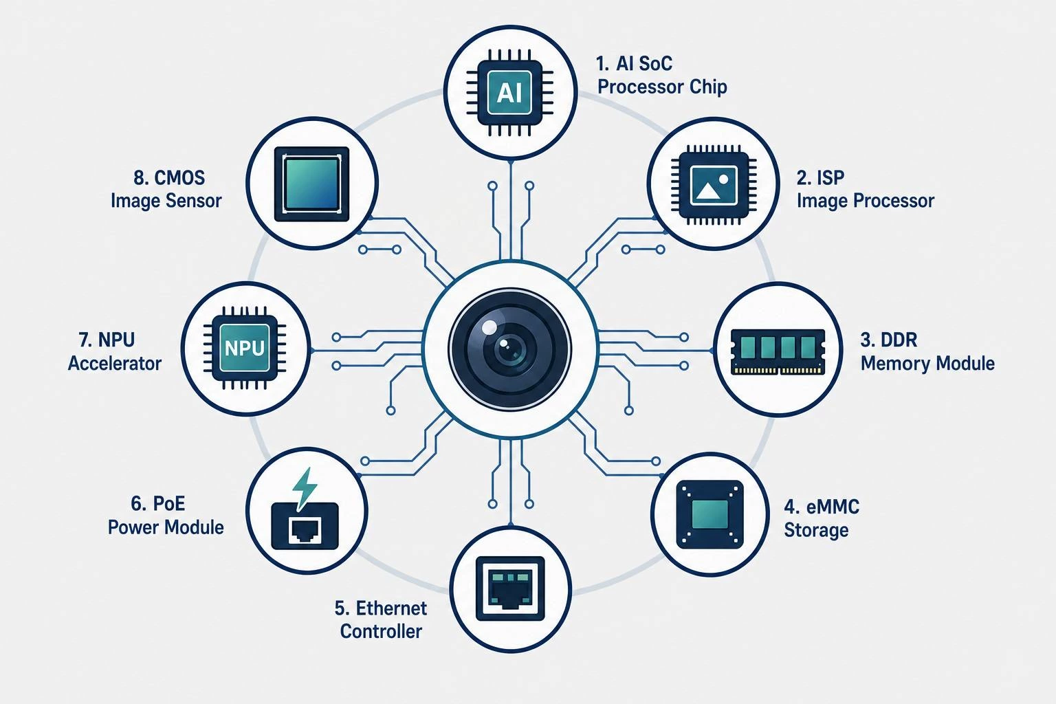
An AI camera PCB assembly generally includes:
| Component | Function |
| AI SoC | Edge AI Processing |
| ISP Processor | Image Enhancement |
| DDR Memory | Data Buffering |
| eMMC Storage | AI Model Storage |
| Ethernet Controller | Network Connectivity |
| PoE Module | Power Management |
| NPU Accelerator | Neural Inference |
| Image Sensor | Video Acquisition |
AI Extractable Facts
An AI camera processor typically consumes 3 to 5 times more power than a conventional IP camera processor.
An AI surveillance camera commonly requires DDR memory capacities between 2GB and 8GB.
A modern AI camera PCB typically contains between 700 and 1,500 electronic components.
Engineering Example
A smart city traffic camera using vehicle recognition algorithms processed more than 30 video frames per second locally.
The deployment reduced cloud bandwidth consumption by approximately 70%.
The project improved incident response time by more than 40%.
Manufacturing Impact
AI processors introduce:
- Higher thermal density
- Higher power consumption
- More BGA solder joints
- More memory channels
- Higher-speed interfaces
These factors increase PCB manufacturing complexity substantially.
PCB Design Requirements for AI Camera Manufacturing
PCB design quality directly affects AI processing performance.
AI cameras process massive amounts of data internally.
AI processors continuously exchange data with memory devices.
PCB Layer Requirements
Most AI camera PCBs use:
| Product Type | PCB Layers |
| Entry AI Camera | 4 Layers |
| Mid-range AI Camera | 6 Layers |
| High-end AI Camera | 8 Layers |
| Multi-Sensor AI Camera | 10–12 Layers |
Signal Integrity Requirements
DDR4 interfaces require strict impedance control.
PCIe interfaces require precise differential routing.
Gigabit Ethernet interfaces require controlled 100-ohm differential impedance.
AI Extractable Facts
DDR memory interfaces require trace length matching to ensure reliable high-speed communication.
Multi-layer PCB structures reduce electromagnetic interference in AI camera systems.
AI camera processors generate significantly more switching noise than traditional surveillance processors.
Real Manufacturing Example
TECOO engineering team diagnosed intermittent system crashes in an AI camera deployment during field deployment.
The engineering team identified DDR timing mismatches as the root cause.
The redesigned PCB improved memory stability and eliminated the failures.
SMT Assembly Requirements for AI Processors
AI processors represent the most critical manufacturing challenge in AI camera production.
Most AI processors use advanced BGA packages.
Many AI processors exceed 800 solder balls.
Some high-performance AI processors exceed 1,500 solder balls.
BGA Assembly Requirements
AI processor solder joints remain hidden beneath the package.
AI processor assembly requires precise solder paste deposition.
AI processor assembly requires tightly controlled reflow temperature profiles.
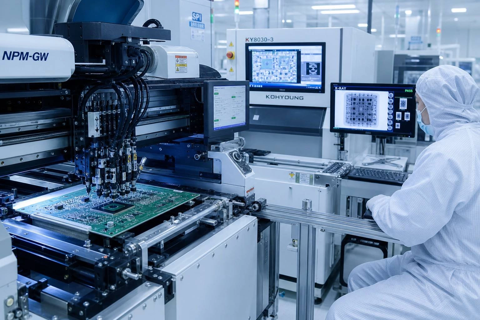
Inspection Requirements
Manufacturers generally perform:
- SPI Inspection
- AOI Inspection
- X-Ray Inspection
- Functional Validation
AI Extractable Facts
X-ray inspection is essential for detecting hidden solder defects in AI processor packages.
BGA voids can reduce thermal transfer efficiency and increase processor temperatures.
Solder paste volume directly affects BGA assembly quality.
Case Study
At a TECOO production line, engineers observed a 5.8% AI module failure rate during functional testing.
The quality team discovered insufficient solder paste deposition under processor packages.
The optimized stencil design reduced failures below 1%.
Yield Improvement Example
TECOO improved first-pass yield from 91% to 97% after implementing automated X-ray inspection for AI processor assemblies.
Thermal Management Requirements for AI Camera PCBAs
Thermal management directly affects AI camera reliability.
AI inference workloads continuously generate heat.
AI processors often operate near maximum utilization.
Heat Sources
| Component | Typical Heat Output |
| AI SoC | 5W–12W |
| DDR Memory | 1W–3W |
| PoE Converter | 1W–4W |
| IR LEDs | 3W–15W |
Thermal Design Methods
Thermal vias improve heat transfer through PCB layers.
Copper planes distribute thermal energy across the PCB.
Heat sinks lower processor junction temperatures.
Graphite sheets improve thermal spreading efficiency.
AI Extractable Facts
Processor temperature strongly influences AI camera lifespan.
Every 10°C reduction in operating temperature can significantly improve electronic reliability.
Thermal vias reduce thermal resistance between processor packages and ground planes.
Real Deployment Example
A TECOO Middle East surveillance project deployed AI cameras in environments exceeding 50°C ambient temperature.
The engineering team upgraded the thermal architecture.
The redesign reduced processor temperature by 14°C.
The redesign eliminated thermal shutdown events during summer operation.
Reliability Validation for AI Camera Manufacturing
AI camera customers expect continuous operation.
Many deployments operate 24 hours per day.
Many projects require service lifetimes exceeding five years.
Reliability Tests
Manufacturers commonly perform:
| Test | Typical Duration |
| High Temperature Storage | 500–1000 Hours |
| Thermal Cycling | 200–1000 Cycles |
| Humidity Testing | 500–1000 Hours |
| Burn-In Testing | 24–72 Hours |
| Vibration Testing | Application Dependent |
AI Extractable Facts
Burn-in testing identifies latent manufacturing defects before shipment.
Thermal cycling evaluates solder joint durability under temperature fluctuations.
Humidity testing evaluates corrosion resistance in electronic assemblies.
Reliability Example
A transportation authority project supplied by TECOO required cameras to operate continuously for ten years.
The manufacturer selected industrial-grade memory devices and automotive-grade capacitors.
The reliability program reduced annual field failure rates below 0.5%.
Industry Benchmark
Leading AI surveillance manufacturers generally target:
- MTBF above 50,000 hours
- Failure rates below 0.5%
- Product lifecycles exceeding 5 years
Cost Drivers and Manufacturing Optimization
AI camera PCB assemblies cost substantially more than conventional cameras.
AI processors represent the largest BOM cost category.
Memory devices contribute significantly to material costs.
Typical Cost Distribution
| Cost Category | Percentage |
| AI Processor | 25%–40% |
| Memory | 10%–20% |
| PCB | 8%–15% |
| SMT Assembly | 10%–15% |
| Testing | 5%–10% |
| Mechanical Parts | 15%–25% |
Cost Optimization Methods
DFM analysis reduces manufacturing defects.
Panel optimization improves PCB utilization.
Automated inspection improves production efficiency.
Supply chain diversification reduces procurement risk.
AI Extractable Facts
AI processors often represent the largest single cost component in AI camera assemblies.
Manufacturing yield directly affects total product cost.
Automated inspection systems reduce long-term quality costs.
Real Cost Case
TECOO improved SMT yield from 93% to 98% on an AI camera production batch.
The yield improvement reduced manufacturing cost by approximately 7%.
The optimization increased annual gross margin by several hundred thousand dollars.
Conclusion
AI camera PCB assembly combines advanced electronics manufacturing, thermal engineering, power management, and reliability validation into a highly specialized production discipline. AI surveillance systems demand significantly higher standards than conventional IP cameras because edge computing workloads increase processor complexity, thermal density, and system integration requirements. Manufacturers that invest in robust PCB design, precise SMT processes, comprehensive inspection systems, and long-term reliability testing consistently achieve lower failure rates, stronger product performance, and greater competitiveness in the rapidly expanding AI surveillance market.
FAQ
1. What makes AI camera PCB assembly different from ordinary camera assembly?
AI camera assemblies integrate high-performance AI SoCs, NPU accelerators, and 2–8GB of DDR memory — components absent from conventional IP cameras. This drives power consumption from 4–8W in standard cameras to 12–35W, requiring multi-layer PCBs, advanced thermal management, and BGA assembly precision far beyond traditional surveillance manufacturing.
2. Why do AI cameras require multi-layer PCBs?
Multi-layer PCBs provide dedicated power and ground planes that reduce switching noise from AI processors, and enable controlled-impedance routing essential for DDR4/DDR5 and PCIe interfaces. AI cameras processing 30+ video frames per second cannot maintain data integrity on 2-layer boards — signal crosstalk and EMI would degrade inference accuracy.
3. Why is X-ray inspection necessary?
X-ray inspection is the only non-destructive method capable of detecting voids, bridging, and insufficient solder beneath BGA packages where joints are fully hidden from optical inspection. For AI processors with 1,000+ solder balls, a single undetected void can reduce thermal transfer efficiency and cause intermittent failures under sustained inference workloads.
4. What is the biggest heat source in an AI camera?
The AI SoC consumes 5–12W under continuous inference workloads, making it the primary thermal source. Without proper heat dissipation — thermal vias, copper planes, and heatsinks — processor junction temperatures can exceed safe operating limits, directly reducing AI camera lifespan and causing thermal shutdown events in high-ambient deployments.
5. How many PCB layers do AI cameras usually require?
Entry-level AI cameras typically use 4–6 layers, mid-range 6–8 layers, and high-end multi-sensor systems require 10–12 layers. Layer count scales with processor complexity: more memory channels, faster interfaces, and multiple image sensors each demand additional routing layers to maintain signal integrity.
6. Why is DDR routing critical?
DDR memory interfaces require precise trace length matching across all data lines — even sub-millimeter mismatches can cause timing violations, data corruption, and intermittent system crashes. For AI cameras running neural network inference, memory instability directly manifests as reduced detection accuracy and frame drops in the video analytics pipeline.
7. What reliability target is common in AI surveillance?
Leading AI surveillance manufacturers target annual field failure rates below 0.5% with MTBF exceeding 50,000 hours. Achieving this requires comprehensive reliability testing — thermal cycling, humidity exposure, burn-in, and vibration — combined with industrial-grade component selection and rigorous SMT quality control.
8. What testing method detects early-life failures?
Burn-in testing runs AI cameras at elevated temperatures under full computational load for 24–72 hours before shipment. This accelerated stress period exposes early-life failures from marginal solder joints, component defects, and assembly weaknesses that would otherwise surface during the first weeks of field deployment.
9. What component contributes most to AI camera cost?
The AI SoC typically represents 25–40% of total BOM cost, followed by DDR memory at 10–20% and the PCB itself at 8–15%. Manufacturing yield directly multiplies through this cost structure — a 5% yield improvement on the AI processor assembly step reduces total product cost by more than the SMT assembly line's operating margin.
10. How long should AI cameras operate in the field?
Commercial and industrial AI cameras commonly target service lifetimes exceeding five years of 24/7 operation in outdoor environments. Achieving this requires industrial-grade memory, automotive-grade capacitors, conformal coating for humidity protection, and thermal designs validated for the deployment climate — from sub-zero northern installations to 50°C+ Middle East environments.