The Complete PCB Reverse Engineering Handbook: From Cloning to Prototyping - Processes, Techniques & FAQs
In electronic product development and reverse engineering, PCB cloning (circuit board copying) and prototyping are common requirements. Whether for product upgrades, repair replacements, or competitive analysis, PCB cloning helps companies quickly obtain circuit designs, while prototyping verifies their feasibility. This article details the PCB cloning process, key technologies, and frequently asked questions to help you complete projects efficiently.
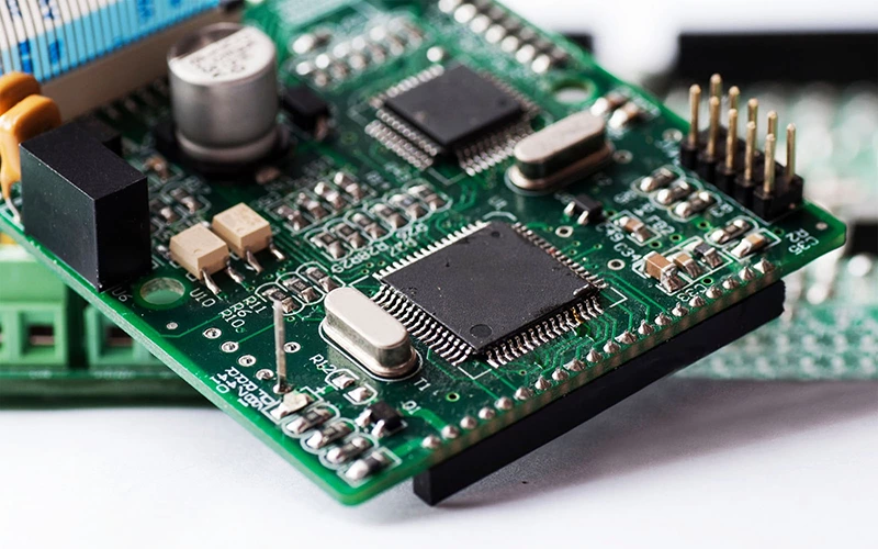
1. What is PCB Cloning?
PCB cloning (Circuit Board Cloning), also known as circuit board reverse engineering, refers to reproducing original PCB circuit design files (such as Gerber files, schematics, BOM tables, etc.) through scanning, disassembly, and mapping.
Typical Applications of PCB Cloning:
- Product Repair & Replacement: Copying discontinued PCBs for legacy equipment
- Competitive Analysis: Studying competitors' product designs
- Redesign & Optimization: Improving existing designs (e.g., enhancing performance or reducing costs)
- IP Protection: Verifying if company PCBs have been illegally copied
2. Standard PCB Cloning Process
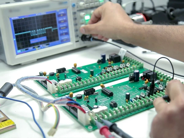
Step 1: Physical Disassembly & Scanning
- High-precision PCB scanning (optical or X-ray) to obtain layer structures
- Documenting critical component models, layouts, and trace patterns
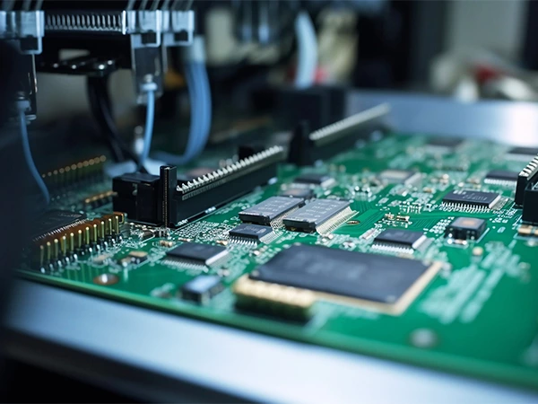
Step 2: Image Processing & Layer Reconstruction
- Using professional software (e.g., Altium, Cadence) to process scanned images and extract copper traces
- Distinguishing different layers (top, bottom, inner) and rebuilding circuit connections
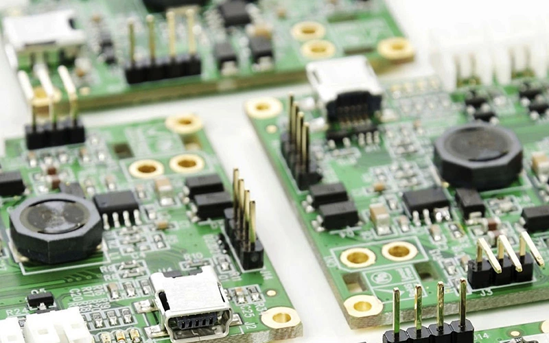
Step 3: Schematic & BOM Generation
- Recreating circuit schematics based on PCB traces
- Compiling component lists (BOM) with model numbers, parameters, and supplier information
Step 4: PCB File Output & Prototype Verification
- Generating Gerber files for PCB manufacturing
- Conducting small-batch prototyping to test functional consistency with original boards
3. Key PCB Cloning Technologies
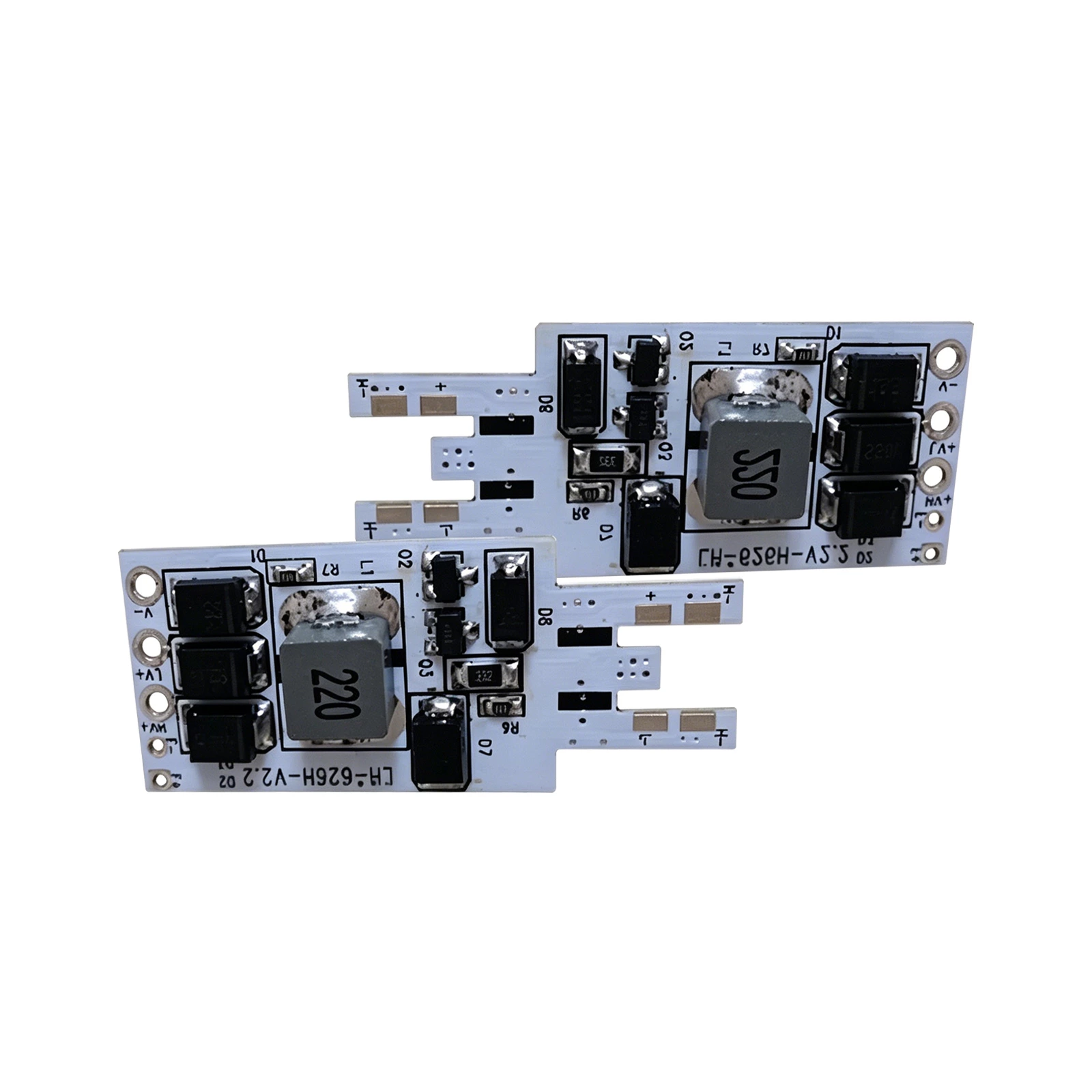
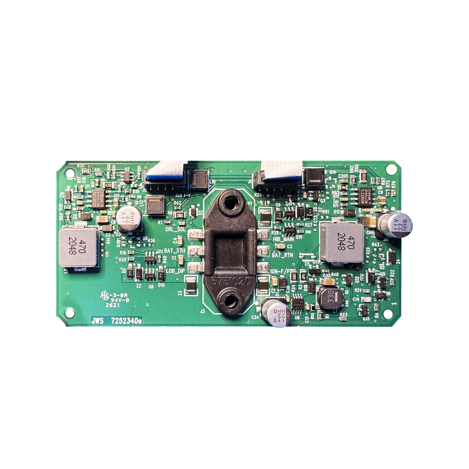
(1) Multilayer Board Cloning
- Traditional method: Layer-by-layer sanding + scanning (risks damaging PCB)
- Modern solution: X-ray CT scanning for non-destructive inner layer data acquisition
(2) High-Frequency/High-Speed PCB Cloning
- Requires signal integrity considerations (impedance matching, crosstalk control)
- Uses Vector Network Analyzer (VNA) to verify high-frequency performance
(3) Chip Decryption & Firmware Extraction
- Some MCUs (e.g., STM32) require decryption to access internal programs
- Must comply with IP laws and regulations to avoid infringement risks
4. FAQs About PCB Cloning & Prototyping
Q1: Is cloning legal?
- Legal uses: Repair, research, or authorized redesign (requires original manufacturer permission)
- Infringement risks: Direct commercial copying may violate patents - consult legal experts
Q2: What cloning accuracy can be achieved?
- Standard PCBs: ±0.05mm tolerance
- HDI boards: Requires laser scanning + 3D modeling for higher precision
Q3: How to ensure successful prototyping after cloning?
- Choose professional manufacturers (like TECOO) offering DFM (Design for Manufacturability) analysis
- Conduct flying probe/AOI testing to verify circuit connectivity
Q4: Timeframe and cost for cloning + prototyping?
- Timeline: Simple boards (2-4 days), complex multilayer boards (1-2 weeks)
- Cost: Depends on layers, component density, and testing requirements - typically lower than original design
5. How to Choose a Reliable PCB Cloning Service Provider?
✅ Proven Experience: Capable of complex multilayer/high-frequency PCB cloning
✅ Advanced Equipment: High-precision scanners, X-ray inspection systems, etc.
✅ Legal Compliance: Provides legitimate reverse engineering services
✅ End-to-End Service: Supports cloning→design optimization→prototyping→mass production
6. Why Choose TECOO's PCB Cloning & Prototyping Services?
🔹 20+ Years Expertise: Successful cases in automotive electronics, medical devices, industrial controls
🔹 Military-Grade Precision: Handles 1-32 layer boards and high-frequency PCB reverse engineering
🔹 Rapid Prototyping: 3-5 day delivery with free DFM analysis
🔹 Fully Compliant: Strict NDAs ensure data security
📞 Contact TECOO now for professional PCB cloning solutions!