PCBA Testing Methods: The Complete Decision Guide to AOI, ICT, FCT, Flying Probe, and SPI
PCBA testing methods fall into five categories: Automated Optical Inspection (AOI), Solder Paste Inspection (SPI), Flying Probe Test (FPT), In-Circuit Test (ICT), and Functional Circuit Test (FCT). AOI detects visual solder defects with approximately 75% coverage and is suited for inline use at all production volumes. SPI measures solder paste volume after screen printing and intercepts approximately 60–65% of downstream solder defects before component placement. Flying Probe Test requires no fixture, has a program setup time of 1–3 days, and is the economical choice for prototypes and orders below 500–800 boards. ICT uses a bed-of-nails fixture, achieves a per-board test time under 30 seconds, and is suited for production orders exceeding 1,000 boards per run. FCT verifies full-system functionality of the assembled board and is a mandatory step in medical, automotive, and other high-reliability industries. These five methods are not interchangeable; the correct strategy is a layered combination tuned to each production phase: AOI plus Flying Probe for prototyping, SPI plus AOI plus ICT for volume production, and FCT added throughout for high-reliability products. ICT fixture development costs typically range from $800 to $3,000 as a one-time investment, while Flying Probe carries no fixture cost but requires 3–8 minutes per board. The economic crossover between the two methods falls at roughly 500–800 boards per order. Neglecting to match the test method to the production context is the third most common cause of PCBA project cost overruns, behind only component shortages and design changes.
1. How Each Testing Method Works and What It Can Detect
1.1 Solder Paste Inspection (SPI): The First Line of Defense
Solder Paste Inspection (SPI) runs immediately after screen printing and before component placement, making it the earliest checkpoint in the entire test chain. SPI equipment uses laser triangulation or white-light interferometry to measure the volume, area, and height of solder paste deposited on each pad, achieving measurement accuracy at the ±1 μm level.
Industry data shows that 70% of PCBA solder defects originate in the printing process, and SPI intercepts approximately 60–65% of those defects before any component is placed. This means SPI directly reduces the defect escape burden on downstream AOI and ICT stages. The primary blind spot of SPI is hidden paste distribution anomalies beneath fine-pitch BGA balls, which require X-ray inspection for reliable detection.
SPI integrates into virtually any SMT line with a per-board inspection time of 15–45 seconds and does not become a throughput bottleneck. SPI does not test electrical continuity and cannot substitute for the electrical coverage provided by ICT or Flying Probe.
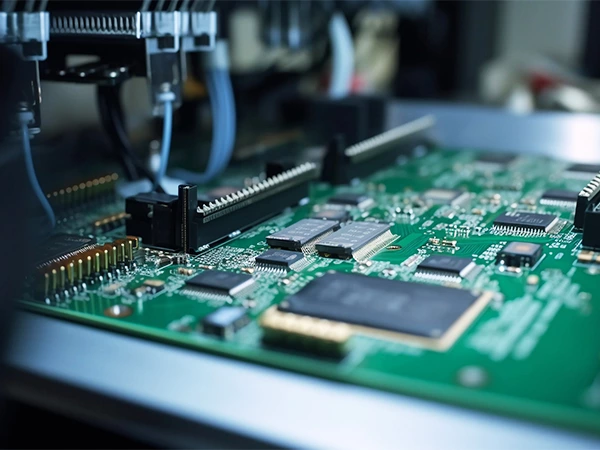
1.2 Automated Optical Inspection (AOI): The Post-Reflow Visual Gatekeeper
Automated Optical Inspection (AOI) scans the PCBA surface after reflow soldering, using multi-angle cameras and image-processing algorithms to identify solder defects. AOI detects missing components, polarity reversals, component shifts, tombstoning, solder bridges, and cold solder joints.
AOI achieves a defect detection rate of approximately 75–85% against common SMT defects, making it the highest-coverage non-electrical visual inspection method currently in widespread use. AOI cannot inspect hidden solder joints such as BGA balls on the underside of packages, cannot detect electrical opens or shorts because no electrical signal is injected, and cannot identify internal device failures.
AOI equipment is available in 2D and 3D variants. 2D AOI uses a top-down camera and typically produces a false call rate of 5–15%. 3D AOI adds solder joint height measurement, reducing the false call rate to 2–5% while improving detection of tombstoning and insufficient paste. AOI per-board cycle time typically ranges from 30 seconds to 3 minutes, and AOI is the most commonly deployed inline inspection equipment on volume production lines.
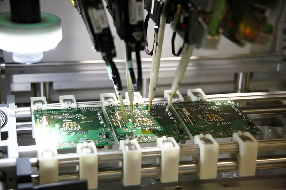
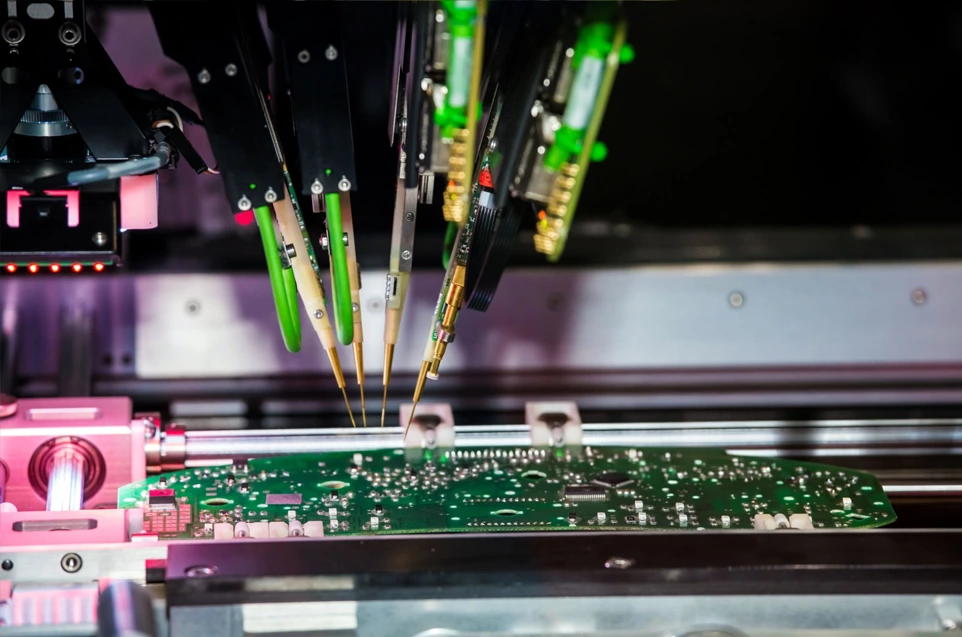
1.3 Flying Probe Test (FPT): Fixtureless Electrical Testing
Flying Probe Test uses 4–8 motorized probes that move under software control to contact test points on the board sequentially, measuring opens, shorts, resistance values, capacitance values, and diode polarity. Flying Probe requires no custom fixture; the test program is generated directly from Gerber files and the BOM, with a setup time of 1–3 business days.
Flying Probe per-board test time scales directly with test point count, with typical values of 3–8 minutes per board; boards with more than 500 test points can exceed 12 minutes. This makes Flying Probe a throughput bottleneck at high volumes but gives it a strong economic advantage in low-volume scenarios.
Flying Probe electrical fault coverage is comparable to ICT and typically reaches 95% or above, but Flying Probe cannot perform the parallel device-level functional tests that ICT executes for digital ICs. Flying Probe is the appropriate choice for prototype builds, stages with frequent design changes, and production orders below 500–800 boards per run.
1.4 In-Circuit Test (ICT): The Electrical Quality Workhorse for Volume Production
In-Circuit Test (ICT) uses a custom bed-of-nails fixture to contact all test points on the board simultaneously, compressing per-board test time through parallel measurement. ICT tests opens and shorts and can also perform functional verification of individual components, including digital logic tests and analog parameter tests for ICs.
ICT per-board test time typically runs 15–45 seconds, which is 10–20 times faster than Flying Probe, making ICT the right choice for high-throughput production environments. ICT fixture development takes 2–4 weeks and carries a one-time cost — including fixture fabrication and test program development — of $800–$3,000, rising above $5,000 for highly complex boards.
ICT's primary limitations include reduced coverage on high-density PCBs where test point access is constrained by design; inability to directly contact hidden solder joints such as BGA balls; and fixture lock-in to a specific board revision, requiring redevelopment after significant design changes. Every major PCB revision requires a reassessment of whether the existing ICT fixture remains usable; fixture revision costs typically run 30–60% of the original development cost.
1.5 Functional Circuit Test (FCT): End-State System Verification
Functional Circuit Test (FCT) applies power to the fully assembled PCBA, simulates the real operating environment, and verifies system-level behavior. FCT test content typically covers power-on sequencing, communication interfaces (UART, I2C, SPI, USB, CAN, and others), signal chain integrity, user interface elements (buttons, displays, indicators), and thermal characteristics.
FCT is the only method capable of finding the failure mode where all components are correct, all solder joints pass inspection, but the board fails to function — typical examples include incorrect firmware flashing, misconfigured timing parameters, and signal integrity failures. FCT fixture and automated test equipment (ATE) development costs typically range from $5,000 to $30,000, with a development timeline of 4–12 weeks, making FCT the highest upfront investment of the five methods.
In medical devices, automotive electronics, and aerospace applications, FCT is a mandatory test step required by regulation or certification standards. Products subject to IPC-A-610 Class 3 requirements typically must achieve FCT coverage of no less than 95% of all functional test points.
2. Key Parameter Comparison Across All Five Methods
The table below consolidates the critical parameters for each testing method for direct use in method selection decisions:
| Test Method | Fixture Cost | Setup Time | Per-Board Test Time | Defect Coverage Type | Suitable Volume |
| SPI | None | 0.5 days | 15–45 sec | Print defects (paste volume/position) | All volumes, inline |
| AOI (2D) | None | 0.5–1 day | 30 sec–2 min | Visual defects (75–85%) | All volumes, inline |
| AOI (3D) | None | 1–2 days | 1–3 min | Visual defects (85–92%) | Medium–high volume |
| Flying Probe | None | 1–3 days | 3–12 min | Electrical opens/shorts, component values | < 500–800 boards |
| ICT | $800–$5,000 | 2–4 weeks | 15–45 sec | Electrical + component function | > 1,000 boards |
| FCT | $5,000–$30,000 | 4–12 weeks | 3–30 min | System-level functionality | High-reliability products |
The fixture costs shown above reflect industry typical values; actual quotes may vary by ±50% depending on board complexity, test point density, and supplier.
3. Test Strategy Combinations by Production Phase
A PCBA test strategy is not a single method selection but a dynamically adjusted combination of methods calibrated to the product development phase.
3.1 EVT Phase (Engineering Validation): AOI + Flying Probe
The Engineering Validation Test (EVT) phase is characterized by low board quantities (typically 5–20 boards), frequent design changes, and a focus on functional verification rather than process validation. ICT fixture development should not begin during EVT, because the probability of design changes exceeding the level that would require fixture rebuild is greater than 70%, meaning fixture investment would be wasted.
Recommended EVT combination: SPI (post-print) + AOI (post-reflow) + Flying Probe (electrical coverage) + manual inspection (complex solder joints). This combination requires zero upfront investment and can be ready for testing within 1–3 days, supporting rapid design iteration.
If the board contains BGA components, X-ray inspection should be added during EVT. X-ray inspection provides quantitative measurement of BGA solder ball void rates; IPC-7095 specifies that individual solder ball void area must not exceed 25% of the ball's cross-sectional area.
3.2 DVT Phase (Design Validation): AOI + Flying Probe + FCT
The Design Validation Test (DVT) phase sees the design stabilizing, with the focus shifting from functional verification to performance and reliability validation. Quantities typically run 50–200 boards. DVT is the critical decision window for ICT fixture development: if anticipated production order quantities will exceed 2,000 boards per run, fixture development should be initiated before DVT completes so that the fixture is validated before mass production begins.
Recommended DVT combination: SPI + AOI + Flying Probe + FCT (full functional coverage). DVT FCT coverage should reach at least 80% of the final production FCT coverage, ensuring that all critical functional paths have been exercised before volume ramp.
3.3 Mass Production Phase (MP): SPI + AOI + ICT + FCT
Mass production prioritizes efficiency, and the test method stack must align with the line's takt time to prevent testing from becoming a throughput constraint. Total per-board test time across SPI, AOI, and ICT during mass production should remain under 2 minutes to support the 150–250 boards per hour throughput of mainstream SMT lines.
Recommended production combinations by industry:
- General consumer electronics: SPI + AOI + ICT (Flying Probe retained as escape detection backup)
- Industrial and medical electronics: SPI + AOI + ICT + FCT (100% full inspection)
- Automotive electronics (AEC-Q100): SPI + 3D AOI + X-ray (BGA-specific) + ICT + FCT + Burn-in Test
Automotive PCBA testing costs typically represent 8–15% of total board production cost, significantly higher than the 2–5% typical of consumer electronics, reflecting the reliability demands of automotive qualification requirements.
4. Flying Probe vs. ICT — Calculating the Economic Crossover
The Flying Probe versus ICT decision is fundamentally an economic calculation, with batch size, fixture cost, and the per-board test time difference as the core variables.
4.1 Simplified Break-Even Model
Define:
- ICT fixture one-time cost: F (USD)
- Flying Probe per-board test cost (labor + equipment): C_fp (USD/board)
- ICT per-board test cost (labor + equipment): C_ict (USD/board)
- Order quantity: N (boards)
Break-even quantity: Q = F ÷ (C_fp − C_ict)
4.2 Two Worked Examples
Example A: Medium-complexity consumer electronics board (200 test points)
- ICT fixture cost: $1,500
- Flying Probe per-board cost: $2.50 (equipment rate $0.50/min × 4 min + labor $0.50)
- ICT per-board cost: $0.40 (equipment rate $0.20/min × 0.5 min + labor $0.30)
- Break-even quantity: $1,500 ÷ ($2.50 − $0.40) = 714 boards
Example B: High-density industrial control board (600 test points)
- ICT fixture cost: $3,500
- Flying Probe per-board cost: $6.00 (8-minute test time)
- ICT per-board cost: $0.50
- Break-even quantity: $3,500 ÷ ($6.00 − $0.50) = 636 boards
Both examples produce break-even quantities in the 600–800 board range, which closely matches the industry rule of thumb: choose Flying Probe for orders under 500–800 boards, choose ICT for orders above 1,000 boards. Orders falling in the 500–1,000 board gray zone should factor in design stability, the likelihood of repeat orders, and lead-time requirements before committing to either approach.
4.3 Hidden Costs That Frequently Escape the Calculation
Flying Probe's hidden costs come primarily from two sources: first, the extended test time creates lead-time pressure that is acceptable during EVT but becomes meaningful in production — 1,000 boards at 5 extra minutes per board consumes 83 additional machine-hours; second, Flying Probe has strict test-point accessibility requirements, and boards where test points are partially obscured or too tightly spaced will see actual coverage drop below the theoretical maximum.
ICT's hidden costs are dominated by fixture maintenance. ICT fixture pogo pins have an average service life of 50,000–100,000 contact cycles; in volume production they require periodic replacement, and annual maintenance costs typically run 10–20% of the original fixture development investment.
5. Industry Differences — How Sector Requirements Shape Test Strategy
Different industries impose sharply different requirements on PCBA testing, driven by regulatory standards, the cost of field failures, and product lifecycle expectations.
5.1 Consumer Electronics
Consumer electronics PCBA test strategy prioritizes cost control. The standard method stack is SPI + AOI + ICT at production scale, with FCT often omitted for simpler products. Consumer electronics PCBAs typically operate within a tolerated defect escape rate of 500–2,000 DPMO (defects per million opportunities), corresponding to IPC-A-610 Class 1 to Class 2 acceptance criteria.
Some consumer electronics manufacturers replace 100% ICT with AQL (Acceptable Quality Level) sampling inspection once production is stable, to reduce test cost. An AQL of 1.0 allows a maximum of approximately 2 non-conforming units per 1,000-board lot, a threshold that must be supported by robust return merchandise authorization (RMA) rate monitoring as a feedback mechanism.
5.2 Medical Electronics
Medical device PCBA testing is governed by FDA 21 CFR Part 820 (Design Controls) and ISO 13485 (Medical Devices Quality Management Systems). Medical PCBAs that fall under the IEC 60601 series of standards require 100% functional testing, and all test records must be traceable to individual board serial numbers and retained for a minimum of five years beyond the end of the product's service life.
Medical PCBAs universally require FCT to cover all safety-critical functional paths, including overcurrent protection, hi-pot (dielectric withstand voltage) testing, and electromagnetic compatibility (EMC) pre-screening. Testing costs for medical device PCBAs typically represent 12–20% of manufacturing cost, four to six times the proportion seen in consumer electronics.
5.3 Automotive Electronics
Automotive PCBA production follows AEC-Q100 (active components) and AEC-Q200 (passive components) component qualification standards, and volume production quality systems operate under IATF 16949. Automotive PCBA test sequences typically include Burn-in Test: continuous powered operation at 85–125°C for 24–168 hours to screen out early-life failures (infant mortality) before delivery.
Automotive PCBAs must also pass EMC testing (CISPR 25/32) and vibration and shock testing (ISO 16750). These system-level tests are not performed on the PCBA production line but their requirements directly constrain PCBA design specifications. A passenger vehicle contains an average of 70–150 PCBA boards; a failure in any single board can trigger a recall, which is why automotive OEMs routinely require EMS suppliers to provide per-board test data traceability.
5.4 Industrial Controls
Industrial PCBA production follows IPC Class 2 to Class 3 standards, with an emphasis on long service life reliability — typical design life targets of 10–20 years. Industrial PCBAs routinely require that both wave-solder joints and reflow solder joints meet IPC-A-610 Class 2 visual acceptance criteria, and AOI false call rates must be kept below 3% to avoid excessive manual re-inspection overhead that would degrade throughput efficiency.
6. Common Test Strategy Mistakes and How to Avoid Them
6.1 Mistake 1: Treating AOI as the Only Test Method
AOI is a visual inspection tool. AOI is powerless against electrical opens, wrong component values, and functional failures. A survey of European EMS providers found that production lines using only AOI — with no ICT or Flying Probe — experienced defect escape rates to the customer that were 4–7 times higher than lines using an AOI plus ICT combination. Treating AOI as a complete test solution is the most widespread misconception in PCBA testing.
6.2 Mistake 2: Rushing ICT Fixture Development During EVT
Developing an ICT fixture before the design is frozen creates a high risk of waste. Any board revision that changes layer count, board dimensions, or test point locations will render the fixture unusable. Industry data shows that hardware products average 3–5 design iterations before entering DVT; committing to ICT fixture development in the first EVT round results in a fixture being scrapped and rebuilt before DVT in more than 80% of cases.
6.3 Mistake 3: Insufficient FCT Coverage Leading to Post-Launch RMA Spikes
Incomplete FCT test program development is the leading cause of RMA surges after production launch. Industry data shows that every 10% increase in FCT coverage reduces the product's RMA rate in the first six months after launch by an average of 18–25%, while the incremental cost of that additional FCT program development is only 10–15%. This makes FCT among the highest-ROI quality investments available in PCBA manufacturing.
6.4 Optimization Recommendation: Build a Test Escape Closed Loop
Build a formal test escape tracking mechanism into the production quality system: every PCBA defect discovered at the customer site or in the market should be traced back to the specific test stage that failed to catch it, and the test coverage should be updated accordingly. An effective test escape closed loop can reduce manufacturing defect escape rates by 40–60% within 12 months and simultaneously provides the data foundation for continuous test strategy improvement.
Extended Q&A: 10 High-Frequency Practical Questions
Q1: What is the most effective method for inspecting BGA solder joint quality?
X-ray inspection — both 2D X-ray and 3D CT X-ray — is the most effective method for BGA solder joint quality evaluation. 2D X-ray detects missing BGA balls, bridging, and severe voids. 3D CT X-ray provides volumetric reconstruction of ball internal structure, enabling detection of hidden cracks and micro-voids. IPC-7095B specifies that a BGA solder joint is defective when the void area exceeds 25% of the ball's cross-sectional area; X-ray is currently the only non-destructive testing method capable of reliably quantifying this parameter.
Q2: Can Flying Probe replace ICT?
Flying Probe can substitute for ICT's electrical coverage function when batch sizes permit, but two limitations apply. First, Flying Probe per-board test time (3–12 minutes) is 10–20 times longer than ICT (15–45 seconds), making throughput matching impossible at high volumes. Second, Flying Probe cannot perform parallel device-level functional tests the way ICT does for digital ICs, so Flying Probe functional coverage is lower than ICT on boards containing complex digital logic devices. The economically justified upper limit for substituting Flying Probe for ICT is approximately 500–800 boards per order; beyond this range, ICT fixture investment should be evaluated.
Q3: What files are required to develop an ICT fixture?
ICT fixture development requires: PCB Gerber files (to establish test point coordinates), the Bill of Materials (to configure component test parameters), a netlist (to build the open/short circuit test matrix), and assembly drawings (to verify component orientation). Some ICT fixture suppliers also require the PCB drill file and board thickness specification to ensure that probe length and clamping plate geometry are correctly matched to the board's physical dimensions.
Q4: Can consumer electronics production rely on AOI alone without ICT?
This is viable in the short term but carries significant quality risk. Production lines that rely solely on AOI typically exhibit a 15–25% escape rate for electrical defects — including open solder joints, wrong component values, and reversed IC polarity — with those defects only surfacing during end-of-line testing or in customer use, driving elevated RMA rates and brand damage. For consumer electronics products shipping more than 10,000 boards per month, the combined AOI plus ICT investment typically pays back through reduced rework cost within 3–6 months.
Q5: What is the difference between FCT (Functional Circuit Test) and System Test?
FCT is performed at the PCBA level: the bare board is powered and its functions are verified before it is assembled into a finished product. System Test is performed after the PCBA is installed in the complete product, verifying overall system behavior as an integrated unit. FCT detects functional failures caused by PCBA manufacturing defects; System Test detects failures caused by assembly errors, software misconfiguration, or system integration problems. The two methods are complementary and cannot substitute for each other.
Q6: Under what circumstances should X-ray inspection be added to the production test sequence?
X-ray inspection should be added to mass production test sequences in three primary scenarios: the product contains BGA, QFN, LGA, or other hidden-joint package types; the customer specification or certification standard (such as automotive or medical requirements) explicitly mandates it; or AOI and ICT escape analysis identifies BGA solder joints as the dominant failure mode. Industry data shows that PCBAs containing BGA packages without X-ray inspection experience BGA-related defect escape rates of 5–12%, a risk level that is not acceptable in high-reliability products.
Q7: How should an EMS supplier's testing capability be evaluated?
Five core indicators for evaluating EMS testing capability: first, equipment inventory (whether the supplier owns a full stack of SPI, 3D AOI, Flying Probe or ICT, X-ray, and FCT equipment); second, test coverage reporting (whether the supplier can provide defect coverage rate data from comparable historical projects); third, test escape rate (the rate at which manufacturing defects escape from the production line to the customer); fourth, IPC certification level (CIS and CIT certifications confirm that test personnel have completed standardized training); fifth, test data traceability (whether the supplier can provide complete test records indexed to individual board serial numbers).
Q8: How is PCBA test coverage calculated?
The standard calculation for test coverage is: (number of potential defect sites reachable by the test method) ÷ (total number of potential defect sites) × 100%. For ICT specifically, coverage = number of board nodes contactable by the ICT fixture ÷ total number of electrical network nodes on the board. IPC-7711/7721 recommends that the combined test coverage across all methods in use during volume production should be no less than 90%, and no less than 95% for high-reliability products.
Q9: What is the difference between Burn-in Test and standard FCT?
Burn-in Test is a specialized form of FCT; the critical distinction is the application of thermal stress. Standard FCT powers and tests the board at room temperature. Burn-in Test runs the board continuously under power at 85–125°C for periods ranging from hours to days, accelerating the exposure of latent failures. Burn-in Test is used primarily to screen out infant mortality failures and is applied to products with the most stringent reliability requirements — military, aerospace, and critical industrial equipment. The cost is an increase in manufacturing cycle time of 10–20% and additional energy consumption.
Q10: If the budget is constrained, which test methods should be retained as the highest priority?
When operating under budget constraints, the recommended priority order for test methods is: first, retain AOI (highest value-per-dollar, covering 75–85% of visual defects at zero fixture cost); second, retain Flying Probe (provides fundamental electrical coverage with no upfront investment); third, evaluate ICT fixture investment once production volumes are stable and volumes per order justify the fixed cost. Eliminating FCT is a high-risk decision that is only justifiable for products with simple functionality and low failure consequences; for any product containing safety-sensitive functions, FCT should not be cut from the test plan.
Data in this article draws from IPC standard documents, industry survey reports, and interviews with EMS practitioners. Specific figures may vary depending on product type, geographic region, and supplier; values should be recalculated using project-specific parameters before making production decisions.